PIC18CXX2
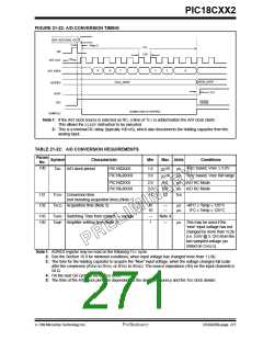
FIGURE 21-22: A/D CONVERSION TIMING
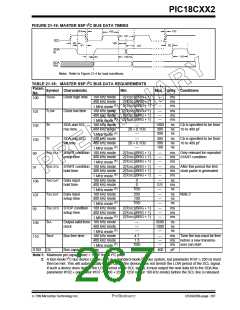
BSF ADCON0, GO
Note 2
131
130
Q4
132
A/D CLK
. . .
. . .
9
8
7
2
1
0
A/D DATA
NEW_DATA
TCY
OLD_DATA
ADRES
ADIF
GO
DONE
SAMPLING STOPPED
SAMPLE
Note 1: If the A/D clock source is selected as RC, a time of TCY is added before the A/D clock starts.
This allows the SLEEPinstruction to be executed.
2: This is a minimal RC delay (typically 100 nS), which also disconnects the holding capacitor from the
analog input.
TABLE 21-22: A/D CONVERSION REQUIREMENTS
Param
Symbol
Characteristic
Min
Max Units
Conditions
No.
20 (5)
130
TOSC based, VREF ≥ 3.0V
TAD
A/D clock period
PIC18CXXX
1.6
3.0
µs
20 (5)
6.0
PIC18LCXXX
µs TOSC based, VREF full range
PIC18CXXX
2.0
3.0
11
µs A/D RC Mode
µs A/D RC Mode
TAD
PIC18LCXXX
9.0
131
132
TCNV Conversion time
12
(not including acquisition time) (Note 1)
TACQ Acquisition time (Note 3)
15
10
—
—
µs -40°C ≤ Temp ≤ 125°C
µs
0°C ≤ Temp ≤ 125°C
135
136
TSWC Switching Time from convert → sample
TAMP Amplifier settling time (Note 2)
—
1
Note 4
—
µs This may be used if the
“new” input voltage has not
changed by more than 1LSb
(i.e. 5 mV @ 5.12V) from the
last sampled voltage (as
stated on CHOLD).
Note 1: ADRES register may be read on the following TCY cycle.
2: See the Section 16.0 for minimum conditions, when input voltage has changed more than 1 LSb.
3: The time for the holding capacitor to acquire the “New” input voltage, when the voltage changes full scale
after the conversion (AVDD to AVSS, or AVSS to AVDD). The source impedance (RS) on the input channels is
50 Ω.
4: On the next Q4 cycle of the device clock.
5: The time of the A/D clock period is dependent on the device frequency and the TAD clock divider.
7/99 Microchip Technology Inc.
Preliminary
DS39026B-page 271

 MICROCHIP [ MICROCHIP ]