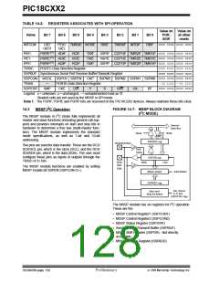
PIC18CXX2
14.2.1.4 MASTER MODE
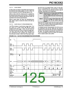
Figure 14-3, Figure 14-5, and Figure 14-6 where the
MSB is transmitted first. In master mode, the SPI clock
rate (bit rate) is user programmable to be one of the fol-
lowing:
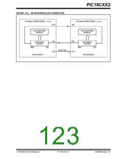
The master can initiate the data transfer at any time
because it controls the SCK. The master determines
when the slave (Processor 2, Figure 14-2) is to broad-
cast data by the software protocol.
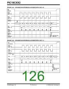
• FOSC/4 (or TCY)
• FOSC/16 (or 4 • TCY)
• FOSC/64 (or 16 • TCY)
• Timer2 output/2
In master mode the data is transmitted/received as
soon as the SSPBUF register is written to. If the SPI is
only going to receive, the SDO output could be disabled
(programmed as an input). The SSPSR register will
continue to shift in the signal present on the SDI pin at
the programmed clock rate. As each byte is received, it
will be loaded into the SSPBUF register as if a normal
received byte (interrupts and status bits appropriately
set). This could be useful in receiver applications as a
“line activity monitor” mode.
This allows a maximum data rate (at 40 MHz) of 10.00
Mbps.
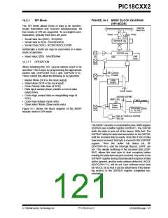
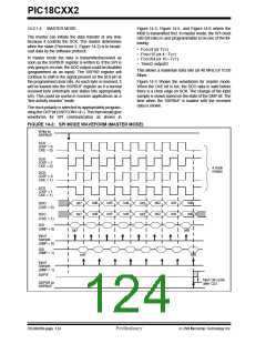
Figure 14-3 Shows the waveforms for master mode.
When the CKE bit is set, the SDO data is valid before
there is a clock edge on SCK. The change of the input
sample is shown based on the state of the SMP bit. The
time when the SSPBUF is loaded with the received
data is shown.
The clock polarity is selected by appropriately program-
ming the CKP bit (SSPCON1<4>). This then would give
waveforms for SPI communication as shown in
FIGURE 14-3: SPI MODE WAVEFORM (MASTER MODE)
Write to
SSPBUF
SCK
(CKP = 0
CKE = 0)
SCK
(CKP = 1
CKE = 0)
4 clock
modes
SCK
(CKP = 0
CKE = 1)
SCK
(CKP = 1
CKE = 1)
bit6
bit6
bit2
bit2
bit5
bit5
bit4
bit4
bit1
bit1
bit0
bit0
SDO
(CKE = 0)
bit7
bit7
bit3
bit3
SDO
(CKE = 1)
SDI
(SMP = 0)
bit0
bit7
Input
Sample
(SMP = 0)
SDI
(SMP = 1)
bit0
bit7
Input
Sample
(SMP = 1)
SSPIF
Next Q4 cycle
after Q2↓
SSPSR to
SSPBUF
DS39026B-page 124
Preliminary
7/99 Microchip Technology Inc.

 MICROCHIP [ MICROCHIP ]