PIC18CXX2
When the application software is expecting to receive
valid data, the SSPBUF should be read before the next
byte of data to transfer is written to the SSPBUF. Buffer
full bit, BF (SSPSTAT<0>), indicates when SSPBUF
has been loaded with the received data (transmission
is complete). When the SSPBUF is read, the BF bit is
cleared. This data may be irrelevant if the SPI is only a
transmitter. Generally the MSSP Interrupt is used to
determine when the transmission/reception has
completed. The SSPBUF must be read and/or written.
If the interrupt method is not going to be used, then
software polling can be done to ensure that a write
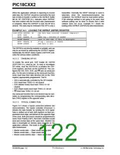
collision does not occur. Example 14-1 shows the
loading of the SSPBUF (SSPSR) for data transmission.
EXAMPLE 14-1: LOADING THE SSPBUF (SSPSR) REGISTER
LOOP BTFSS SSPSTAT, BF
GOTO LOOP
;Has data been received (transmit complete)?
;No
MOVF SSPBUF, W
;WREG reg = contents of SSPBUF
MOVWF RXDATA
;Save in user RAM, if data is meaningful
MOVF TXDATA, W
MOVWF SSPBUF
;W reg = contents of TXDATA
;New data to xmit
The SSPSR is not directly readable or writable, and can
only be accessed by addressing the SSPBUF register.
Additionally, the MSSP status register (SSPSTAT) indi-
cates the various status conditions.
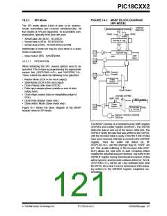
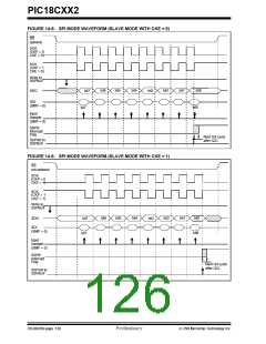
14.2.1.2 ENABLING SPI I/O
To enable the serial port, SSP Enable bit, SSPEN
(SSPCON1<5>), must be set. To reset or reconfigure
SPI mode, clear the SSPEN bit, re-initialize the SSP-
CON registers, and then set the SSPEN bit. This con-
figures the SDI, SDO, SCK, and SS pins as serial port
pins. For the pins to behave as the serial port function,
some must have their data direction bits (in the TRIS
register) appropriately programmed. That is:
• SDI is automatically controlled by the SPI module
• SDO must have TRISC<5> bit cleared
• SCK (Master mode) must have TRISC<3> bit
cleared
• SCK (Slave mode) must have TRISC<3> bit set
• SS must have TRISC<4> bit set
Any serial port function that is not desired may be over-
ridden by programming the corresponding data direc-
tion (TRIS) register to the opposite value.
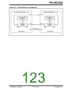
14.2.1.3 TYPICAL CONNECTION
Figure 14-2 shows a typical connection between two
microcontrollers. The master controller (Processor 1)
initiates the data transfer by sending the SCK signal.
Data is shifted out of both shift registers on their pro-
grammed clock edge, and latched on the opposite edge
of the clock. Both processors should be programmed to
same Clock Polarity (CKP), then both controllers would
send and receive data at the same time. Whether the
data is meaningful (or dummy data) depends on the
application software. This leads to three scenarios for
data transmission:
• Master sends data — Slave sends dummy data
• Master sends data — Slave sends data
• Master sends dummy data — Slave sends data
DS39026B-page 122
Preliminary
7/99 Microchip Technology Inc.

 MICROCHIP [ MICROCHIP ]