PIC18CXX2
14.2.1
SPI Mode
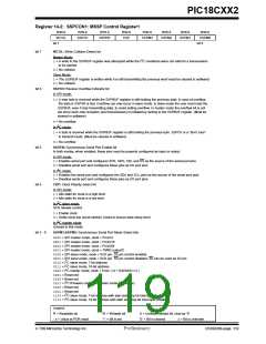
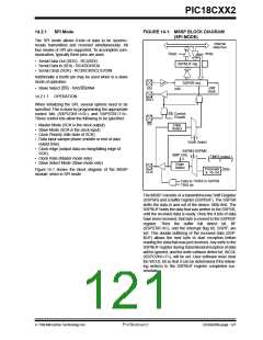
FIGURE 14-1: MSSP BLOCK DIAGRAM
(SPI MODE)
The SPI mode allows 8-bits of data to be synchro-
nously transmitted and received simultaneously. All
four modes of SPI are supported. To accomplish com-
munication, typically three pins are used:
Internal
data bus
Read
Write
• Serial Data Out (SDO) - RC5/SDO
• Serial Data In (SDI) - RC4/SDI/SDA
• Serial Clock (SCK) - RC3/SCK/SCL/LVOIN
SSPBUF reg
SSPSR reg
Additionally a fourth pin may be used when in a slave
mode of operation:
shift
clock
• Slave Select (SS) - RA5/SS/AN4
14.2.1.1 OPERATION
SDI
bit0
SDO
When initializing the SPI, several options need to be
specified. This is done by programming the appropriate
control bits (SSPCON1<5:0>) and SSPSTAT<7:6>.
These control bits allow the following to be specified:
Control
Enable
SS
SS
• Master Mode (SCK is the clock output)
• Slave Mode (SCK is the clock input)
• Clock Polarity (Idle state of SCK)
• Data input sample phase (middle or end of data
output time)
Edge
Select
2
Clock Select
• Clock edge (output data on rising/falling edge of
SCK)
• Clock Rate (Master mode only)
• Slave Select Mode (Slave mode only)
SSPM3:SSPM0
SMP:CKE
2
4
TMR2 output
(
)
2
Edge
Select
TOSC
Prescaler
4, 16, 64
Figure 14-1 shows the block diagram of the MSSP
module, when in SPI mode.
SCK
Data to TX/RX in SSPSR
TRIS bit
The MSSP consists of a transmit/receive Shift Register
(SSPSR) and a buffer register (SSPBUF). The SSPSR
shifts the data in and out of the device, MSb first. The
SSPBUF holds the data that was written to the SSPSR,
until the received data is ready. Once the 8 bits of data
have been received, that byte is moved to the SSPBUF
register. Then the buffer full detect bit, BF
(SSPSTAT<0>), and the interrupt flag bit, SSPIF, are
set. This double buffering of the received data (SSP-
BUF) allows the next byte to start reception before
reading the data that was just received. Any write to the
SSPBUF register during transmission/reception of data
will be ignored, and the write collision detect bit, WCOL
(SSPCON1<7>), will be set. User software must clear
the WCOL bit so that it can be determined if the follow-
ing write(s) to the SSPBUF register completed suc-
cessfully.
7/99 Microchip Technology Inc.
Preliminary
DS39026B-page 121

 MICROCHIP [ MICROCHIP ]