PIC18CXX2
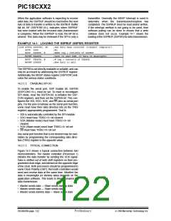
14.2
Control Registers
The MSSP module has three associated registers.
These include a status register and two control regis-
ters.
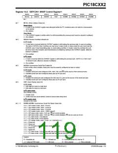
Register 14-1: SSPSTAT: MSSP Status Register
R/W-0
R/W-0
R-0
R-0
R-0
S
R-0
R-0
UA
R-0
BF
SMP
CKE
D/A
P
R/W
bit 7
bit 0
bit 7
SMP: Sample bit
SPI Master Mode
1= Input data sampled at end of data output time
0= Input data sampled at middle of data output time
SPI Slave Mode
SMP must be cleared when SPI is used in slave mode
2
In I C master or slave mode:
1= Slew rate control disabled for standard speed mode (100 kHz and 1 MHz)
0= Slew rate control enabled for high speed mode (400 kHz)
bit 6
CKE: SPI Clock Edge Select
CKP = 0
1= Data transmitted on rising edge of SCK
0= Data transmitted on falling edge of SCK
CKP = 1
1= Data transmitted on falling edge of SCK
0= Data transmitted on rising edge of SCK
2
bit 5
bit 4
D/A: Data/Address bit (I C mode only)
1= Indicates that the last byte received or transmitted was data
0= Indicates that the last byte received or transmitted was address
P: Stop bit
2
(I C mode only. This bit is cleared when the MSSP module is disabled, SSPEN is cleared)
1= Indicates that a stop bit has been detected last (this bit is ’0’ on RESET)
0= Stop bit was not detected last
bit 3
bit 2
S: Start bit
2
(I C mode only. This bit is cleared when the MSSP module is disabled, SSPEN is cleared)
1= Indicates that a start bit has been detected last (this bit is ’0’ on RESET)
0= Start bit was not detected last
2
R/W: Read/Write bit information (I C mode only)
This bit holds the R/W bit information following the last address match. This bit is only valid from the address
match to the next start bit, stop bit, or not ACK bit.
2
In I C slave mode:
1= Read
0= Write
2
In I C master mode:
1= Transmit is in progress
0= Transmit is not in progress.
OR-ing this bit with SEN, RSEN, PEN, RCEN, or ACKEN will indicate if the MSSP is in IDLE mode.
2
bit 1
bit 0
UA: Update Address (10-bit I C mode only)
1= Indicates that the user needs to update the address in the SSPADD register
0= Address does not need to be updated
BF: Buffer Full Status bit
2
Receive (SPI and I C modes)
1= Receive complete, SSPBUF is full
0= Receive not complete, SSPBUF is empty
2
Transmit (I C mode only)
1= Data Transmit in progress (does not include the ACK and stop bits), SSPBUF is full
0= Data Transmit complete (does not include the ACK and stop bits), SSPBUF is empty
Legend:
R = Readable bit
W = Writable bit
U = Unimplemented bit, read as ‘0’
’0’ = Bit is cleared x = Bit is unknown
- n = Value at POR reset
’1’ = Bit is set
DS39026B-page 118
Preliminary
7/99 Microchip Technology Inc.

 MICROCHIP [ MICROCHIP ]