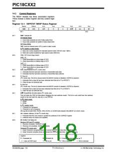
PIC18CXX2
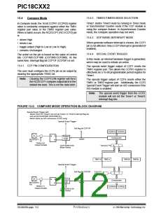
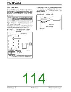
A PWM output (Figure 13-4) has a time base (period)
and a time that the output stays high (duty cycle).
The frequency of the PWM is the inverse of the
period (1/period).
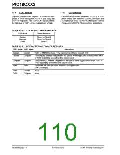
13.5
PWM Mode
In Pulse Width Modulation (PWM) mode, the CCP1 pin
produces up to a 10-bit resolution PWM output. Since
the CCP1 pin is multiplexed with the PORTC data latch,
the TRISC<2> bit must be cleared to make the CCP1
pin an output.
FIGURE 13-4: PWM OUTPUT
Note: Clearing the CCP1CON register will force
the CCP1 PWM output latch to the default
low level. This is not the PORTC I/O data
latch.
Period
Duty Cycle
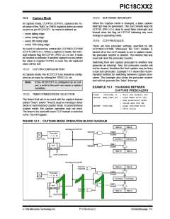
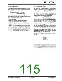
Figure 13-3 shows a simplified block diagram of the
CCP module in PWM mode.
TMR2 = PR2
For a step by step procedure on how to set up the CCP
module for PWM operation, see Section 13.5.3.
TMR2 = Duty Cycle
TMR2 = PR2
FIGURE 13-3: SIMPLIFIED PWM BLOCK
DIAGRAM
CCP1CON<5:4>
Duty cycle registers
CCPR1L
CCPR1H (Slave)
Q
R
S
Comparator
RC2/CCP1
(Note 1)
TMR2
TRISC<2>
Comparator
PR2
Clear Timer,
CCP1 pin and
latch D.C.
Note: 8-bit timer is concatenated with 2-bit internal Q clock
or 2 bits of the prescaler to create 10-bit time-base.
DS39026B-page 114
Preliminary
7/99 Microchip Technology Inc.

 MICROCHIP [ MICROCHIP ]