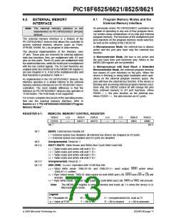
PIC18F6525/6621/8525/8621
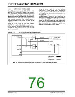
Flash and SRAM devices use different control signal
combinations to implement Byte Select mode. JEDEC
6.2.3
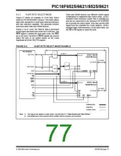
16-BIT BYTE SELECT MODE
Figure 6-3 shows an example of 16-bit Byte Select
mode for PIC18F8525/8621 devices. This mode allows
table write operations to word-wide external memories
with byte selection capability. This generally includes
both word-wide Flash and SRAM devices.
standard Flash memories require that a controller I/O
port pin be connected to the memory’s BYTE/WORD
pin to provide the select signal. They also use the BA0
signal from the controller as a byte address. JEDEC
standard static RAM memories, on the other hand, use
the UB or LB signals to select the byte.
During a TBLWTcycle, the TABLAT data is presented
on the upper and lower byte of the AD15:AD0 bus. The
WRH signal is strobed for each write cycle; the WRL
pin is not used. The BA0 or UB/LB signals are used to
select the byte to be written based on the Least
Significant bit of the TBLPTR register.
FIGURE 6-3:
16-BIT BYTE SELECT MODE EXAMPLE
PIC18F8X2X
AD<7:0>
A<20:1>
373
373
JEDEC Word
Flash Memory
A<x:1>
D<15:0>
D<15:0>
(2)
138
CE
A0
AD<15:8>
(1)
ALE
A<19:16>
OE
BYTE/WORD OE WR
WRH
A<20:1>
WRL
JEDEC Word
A<x:1>
SRAM Memory
BA0
I/O
D<15:0>
D<15:0>
CE
LB
LB
(1)
UB
OE WR
UB
Address Bus
Data Bus
Control Lines
Note 1: This signal only applies to table writes. See Section 5.1 “Table Reads and Table Writes”.
2: Demultiplexing is only required when multiple memory devices are accessed.
2005 Microchip Technology Inc.
DS39612B-page 75

 MICROCHIP [ MICROCHIP ]