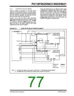
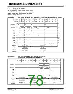
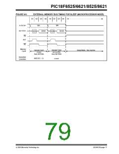
PIC18F6525/6621/8525/8621
During
a
TBLWT cycle to an odd address
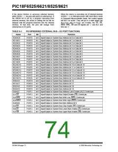
6.2.2
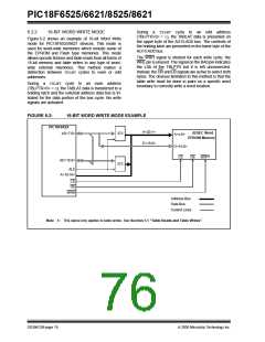
16-BIT WORD WRITE MODE
(TBLPTR<0> = 1), the TABLAT data is presented on
the upper byte of the AD15:AD0 bus. The contents of
the holding latch are presented on the lower byte of the
AD15:AD0 bus.
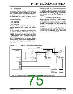
Figure 6-2 shows an example of 16-bit Word Write
mode for PIC18F8525/8621 devices. This mode is
used for word-wide memories which include some of
the EPROM and Flash type memories. This mode
allows opcode fetches and table reads from all forms of
16-bit memory and table writes to any type of word-
wide external memories. This method makes a
distinction between TBLWT cycles to even or odd
addresses.
The WRH signal is strobed for each write cycle; the
WRL pin is unused. The signal on the BA0 pin indicates
the LSb of the TBLPTR but it is left unconnected.
Instead, the UB and LB signals are active to select both
bytes. The obvious limitation to this method is that the
table write must be done in pairs on a specific word
boundary to correctly write a word location.
During
a
TBLWT cycle to an even address
(TBLPTR<0> = 0), the TABLAT data is transferred to a
holding latch and the external address data bus is tri-
stated for the data portion of the bus cycle. No write
signals are activated.
FIGURE 6-2:
16-BIT WORD WRITE MODE EXAMPLE
PIC18F8X2X
AD<7:0>
A<20:1>
D<15:0>
JEDEC Word
EPROM Memory
373
373
A<x:0>
D<15:0>
CE
(1)
OE
WR
AD<15:8>
ALE
A<19:16>
CE
OE
WRH
Address Bus
Data Bus
Control Lines
Note 1: This signal only applies to table writes. See Section 5.1 “Table Reads and Table Writes”.
DS39612B-page 74
2005 Microchip Technology Inc.

 MICROCHIP [ MICROCHIP ]