PIC18F6525/6621/8525/8621
If the device fetches or accesses external memory
while EBDIS = 1, the pins will switch to external bus. If
the EBDIS bit is set by a program executing from
external memory, the action of setting the bit will be
delayed until the program branches into the internal
memory. At that time, the pins will change from
external bus to I/O ports.
When the device is executing out of internal memory
(EBDIS = 0) in Microprocessor with Boot Block mode
or Extended Microcontroller mode, the control signals
will NOT be active. They will go to a state where the
AD<15:0> and A<19:16> are tri-state; the CE, OE,
WRH, WRL, UB and LB signals are ‘1’ and ALE and
BA0 are ‘0’.
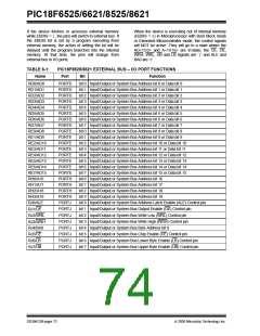
TABLE 6-1:
Name
PIC18F8525/8621 EXTERNAL BUS – I/O PORT FUNCTIONS
Port
Bit
Function
RD0/AD0
RD1/AD1
RD2/AD2
RD3/AD3
RD4/AD4
RD5/AD5
RD6/AD6
RD7/AD7
RE0/AD8
RE1/AD9
RE2/AD10
RE3/AD11
RE4/AD12
RE5/AD13
RE6/AD14
RE7/AD15
RH0/A16
RH1/A17
RH2/A18
RH3/A19
RJ0/ALE
RJ1/OE
PORTD
PORTD
PORTD
PORTD
PORTD
PORTD
PORTD
PORTD
PORTE
PORTE
PORTE
PORTE
PORTE
PORTE
PORTE
PORTE
PORTH
PORTH
PORTH
PORTH
PORTJ
PORTJ
PORTJ
PORTJ
PORTJ
PORTJ
PORTJ
PORTJ
bit 0 Input/Output or System Bus Address bit 0 or Data bit 0
bit 1 Input/Output or System Bus Address bit 1 or Data bit 1
bit 2 Input/Output or System Bus Address bit 2 or Data bit 2
bit 3 Input/Output or System Bus Address bit 3 or Data bit 3
bit 4 Input/Output or System Bus Address bit 4 or Data bit 4
bit 5 Input/Output or System Bus Address bit 5 or Data bit 5
bit 6 Input/Output or System Bus Address bit 6 or Data bit 6
bit 7 Input/Output or System Bus Address bit 7 or Data bit 7
bit 0 Input/Output or System Bus Address bit 8 or Data bit 8
bit 1 Input/Output or System Bus Address bit 9 or Data bit 9
bit 2 Input/Output or System Bus Address bit 10 or Data bit 10
bit 3 Input/Output or System Bus Address bit 11 or Data bit 11
bit 4 Input/Output or System Bus Address bit 12 or Data bit 12
bit 5 Input/Output or System Bus Address bit 13 or Data bit 13
bit 6 Input/Output or System Bus Address bit 14 or Data bit 14
bit 7 Input/Output or System Bus Address bit 15 or Data bit 15
bit 0 Input/Output or System Bus Address bit 16
bit 1 Input/Output or System Bus Address bit 17
bit 2 Input/Output or System Bus Address bit 18
bit 3 Input/Output or System Bus Address bit 19
bit 0 Input/Output or System Bus Address Latch Enable (ALE) Control pin
bit 1 Input/Output or System Bus Output Enable (OE) Control pin
bit 2 Input/Output or System Bus Write Low (WRL) Control pin
bit 3 Input/Output or System Bus Write High (WRH) Control pin
bit 4 Input/Output or System Bus Byte Address bit 0
RJ2/WRL
RJ3/WRH
RJ4/BA0
RJ5/CE
bit 5 Input/Output or System Bus Chip Enable (CE) Control pin
bit 6 Input/Output or System Bus Lower Byte Enable (LB) Control pin
bit 7 Input/Output or System Bus Upper Byte Enable (UB) Control pin
RJ6/LB
RJ7/UB
DS39612B-page 72
2005 Microchip Technology Inc.

 MICROCHIP [ MICROCHIP ]