PIC18F6525/6621/8525/8621
7.1
EEADR and EEADRH
7.0
DATA EEPROM MEMORY
The address register pair can address up to a
maximum of 1024 bytes of data EEPROM. The two
Most Significant bits of the address are stored in
EEADRH, while the remaining eight Least Significant
bits are stored in EEADR. The six Most Significant bits
of EEADRH are unused and are read as ‘0’.
The data EEPROM is readable and writable during
normal operation over the entire VDD range. The data
memory is not directly mapped in the register file
space. Instead, it is indirectly addressed through the
Special Function Registers (SFR).
There are five SFRs used to read and write the
program and data EEPROM memory. These registers
are:
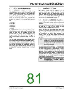
7.2
EECON1 and EECON2 Registers
• EECON1
• EECON2
• EEDATA
• EEADRH
• EEADR
EECON1 is the control register for EEPROM memory
accesses.
EECON2 is not a physical register. Reading EECON2
will read all ‘0’s. The EECON2 register is used
exclusively in the EEPROM write sequence.
Control bits RD and WR initiate read and write
operations, respectively. These bits cannot be cleared,
only set in software. They are cleared in hardware at
the completion of the read or write operation. The
inability to clear the WR bit in software prevents the
The EEPROM data memory allows byte read and write.
When interfacing to the data memory block, EEDATA
holds the 8-bit data for read/write. EEADR and
EEADRH hold the address of the EEPROM location
being accessed. These devices have 1024 bytes of
data EEPROM with an address range from 00h to
3FFh.
accidental or premature termination of
operation.
a write
Note:
During normal operation, the WRERR bit
is read as ‘1’. This can indicate that a write
operation was prematurely terminated by
The EEPROM data memory is rated for high erase/
write cycles. A byte write automatically erases the loca-
tion and writes the new data (erase-before-write). The
write time is controlled by an on-chip timer. The write
time will vary with voltage and temperature, as well as
from chip-to-chip. Please refer to parameter D122
(Section 27.0 “Electrical Characteristics”) for exact
limits.
a
Reset, or
a write operation was
attempted improperly.
The WREN bit, when set, will allow a write operation.
On power-up, the WREN bit is clear. The WRERR bit is
set when a write operation is interrupted by a MCLR
Reset or a WDT Time-out Reset during normal
operation. In these situations, the user can check the
WRERR bit and rewrite the location. It is necessary to
reload the data and address registers (EEDATA and
EEADR) due to the Reset condition forcing the
contents of the registers to zero.
Note:
Interrupt flag bit, EEIF in the PIR2 register,
is set when write is complete. It must be
cleared in software.
2005 Microchip Technology Inc.
DS39612B-page 79

 MICROCHIP [ MICROCHIP ]