PIC18F6525/6621/8525/8621
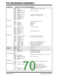
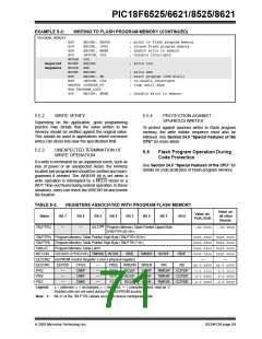
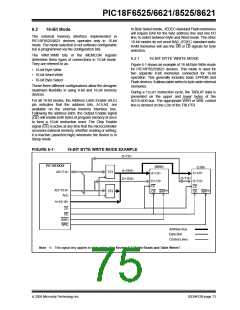
EXAMPLE 5-3:
WRITING TO FLASH PROGRAM MEMORY (CONTINUED)
PROGRAM_MEMORY
BSF
BCF
BSF
BCF
MOVLW
MOVWF
MOVLW
MOVWF
BSF
EECON1, EEPGD
EECON1, CFGS
EECON1, WREN
INTCON, GIE
55h
EECON2
AAh
EECON2
EECON1, WR
INTCON, GIE
; point to Flash program memory
; access Flash program memory
; enable write to memory
; disable interrupts
Required
Sequence
; write 55h
; write AAh
; start program (CPU stall)
; re-enable interrupts
; loop until done
BSF
DECFSZ COUNTER_HI
BRA PROGRAM_LOOP
BCF
EECON1, WREN
; disable write to memory
5.5.2
WRITE VERIFY
5.5.4
PROTECTION AGAINST
SPURIOUS WRITES
Depending on the application, good programming
practice may dictate that the value written to the
memory should be verified against the original value.
This should be used in applications where excessive
writes can stress bits near the specification limit.
To protect against spurious writes to Flash program
memory, the write initiate sequence must also be
followed. See Section 24.0 “Special Features of the
CPU” for more detail.
5.5.3
UNEXPECTED TERMINATION OF
WRITE OPERATION
5.6
Flash Program Operation During
Code Protection
If a write is terminated by an unplanned event, such as
loss of power or an unexpected Reset, the memory
location just programmed should be verified and repro-
grammed if needed. The WRERR bit is set when a
write operation is interrupted by a MCLR Reset or a
WDT Time-out Reset during normal operation. In these
situations, users can check the WRERR bit and rewrite
the location.
See Section 24.0 “Special Features of the CPU” for
details on code protection of Flash program memory.
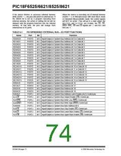
TABLE 5-2:
Name
REGISTERS ASSOCIATED WITH PROGRAM FLASH MEMORY
Value on
Value on:
POR, BOR
Bit 7
Bit 6
Bit 5
Bit 4
Bit 3
Bit 2
Bit 1
Bit 0
all other
Resets
(1)
TBLPTRU
—
—
bit 21
Program Memory Table Pointer Upper Byte
(TBLPTR<20:16>)
--00 0000 --00 0000
TBLPTRH Program Memory Table Pointer High Byte (TBLPTR<15:8>)
TBLPTRL Program Memory Table Pointer High Byte (TBLPTR<7:0>)
0000 0000 0000 0000
0000 0000 0000 0000
0000 0000 0000 0000
0000 000x 0000 000u
TABLAT
INTCON
EECON2
EECON1
IPR2
Program Memory Table Latch
GIE/GIEH PEIE/GIEL TMR0IE INT0IE
RBIE
TMR0IF
INT0IF
RBIF
RD
EEPROM Control Register 2 (not a physical register)
—
—
EEPGD
CFGS
CMIP
CMIF
CMIE
—
—
—
—
FREE
EEIP
EEIF
EEIE
WRERR WREN
WR
xx-0 x000 uu-0 u000
—
—
—
BCLIP
BCLIF
BCLIE
LVDIP
LVDIF
LVDIE
TMR3IP
TMR3IF
TMR3IE
CCP2IP -1-1 1111 -1-1 1111
CCP2IF -0-0 0000 -0-0 0000
PIR2
PIE2
CCP2IE -0-0 0000 -0-0 0000
Legend:
x= unknown, u= unchanged, r= reserved, — = unimplemented, read as ‘0’.
Shaded cells are not used during Flash/EEPROM access.
Note 1: Bit 21 of the TBLPTRU allows access to device configuration bits.
2005 Microchip Technology Inc.
DS39612B-page 69

 MICROCHIP [ MICROCHIP ]