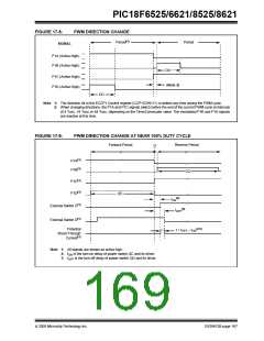
PIC18F6525/6621/8525/8621
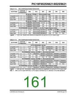
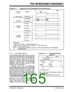
FIGURE 17-3:
PWM OUTPUT RELATIONSHIPS (ACTIVE-LOW STATE)
0
PR2 + 1
Duty
SIGNAL
CCP1CON
Cycle
<7:6>
Period
P1A Modulated
P1A Modulated
P1B Modulated
P1A Active
(Single Output)
00
10
(1)
(1)
Delay
Delay
(Half-Bridge)
P1B Inactive
P1C Inactive
P1D Modulated
P1A Inactive
P1B Modulated
P1C Active
(Full-Bridge,
Forward)
01
(Full-Bridge,
Reverse)
11
P1D Inactive
Relationships:
•
•
•
Period = 4 * TOSC * (PR2 + 1) * (TMR2 Prescale Value)
Duty Cycle = TOSC * (CCPR1L<7:0>:CCP1CON<5:4>) * (TMR2 Prescale Value)
Delay = 4 * TOSC * (ECCP1DEL<6:0>)
Note 1: Dead-band delay is programmed using the ECCP1DEL register (Section 17.4.6 “Programmable
Dead-Band Delay”).
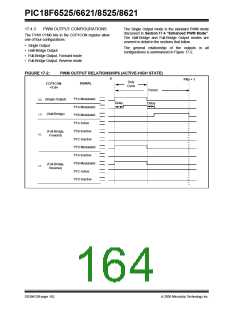
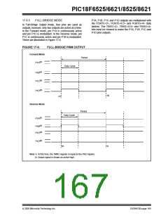
17.4.4
HALF-BRIDGE MODE
FIGURE 17-4:
HALF-BRIDGE PWM
OUTPUT
In the Half-Bridge Output mode, two pins are used as
outputs to drive push-pull loads. The PWM output sig-
nal is output on the P1A pin, while the complementary
PWM output signal is output on the P1B pin
(Figure 17-4). This mode can be used for half-bridge
applications, as shown in Figure 17-5, or for full-bridge
applications, where four power switches are being
modulated with two PWM signals.
Period
Period
Duty Cycle
(2)
(2)
P1A
td
td
P1B
In Half-Bridge Output mode, the programmable
dead-band delay can be used to prevent shoot-through
current in half-bridge power devices. The value of bits
PDC6:PDC0 sets the number of instruction cycles
before the output is driven active. If the value is greater
than the duty cycle, the corresponding output remains
inactive during the entire cycle. See Section 17.4.6
“Programmable Dead-Band Delay” for more details
on dead-band delay operations.
(1)
(1)
(1)
td = Dead Band Delay
Note 1: At this time, the TMR2 register is equal to the
PR2 register.
2: Output signals are shown as active-high.
Since the P1A and P1B outputs are multiplexed with
the PORTC<2> and PORTE<6> data latches, the
TRISC<2> and TRISE<6> bits must be cleared to
configure P1A and P1B as outputs.
2005 Microchip Technology Inc.
DS39612B-page 163

 MICROCHIP [ MICROCHIP ]