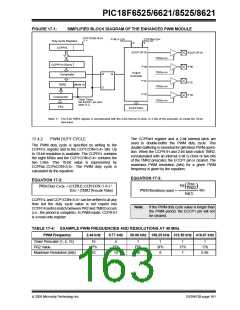
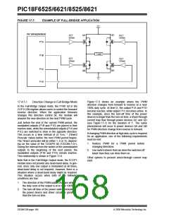
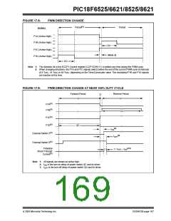
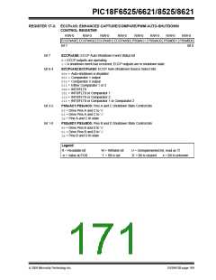
PIC18F6525/6621/8525/8621
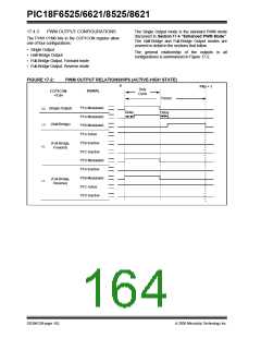
P1A, P1B, P1C and P1D outputs are multiplexed with
the PORTC<2>, PORTE<6:5> and PORTG<4> data
latches. The TRISC<2>, TRISC<6:5> and TRISG<4>
bits must be cleared to make the P1A, P1B, P1C and
P1D pins outputs.
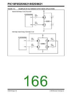
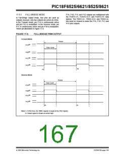
17.4.5
FULL-BRIDGE MODE
In Full-Bridge Output mode, four pins are used as
outputs; however, only two outputs are active at a time.
In the Forward mode, pin P1A is continuously active
and pin P1D is modulated. In the Reverse mode, pin
P1C is continuously active and pin P1B is modulated.
These are illustrated in Figure 17-6.
FIGURE 17-6:
FULL-BRIDGE PWM OUTPUT
Forward Mode
Period
(2)
P1A
Duty Cycle
(2)
(2)
P1B
P1C
(2)
P1D
(1)
(1)
Reverse Mode
Period
Duty Cycle
(2)
P1A
(2)
P1B
(2)
P1C
(2)
P1D
(1)
(1)
Note 1: At this time, the TMR2 register is equal to the PR2 register.
Note 2: Output signal is shown as active-high.
2005 Microchip Technology Inc.
DS39612B-page 165

 MICROCHIP [ MICROCHIP ]