PIC18F6525/6621/8525/8621
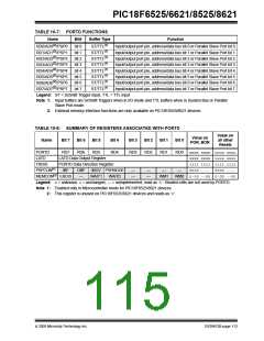
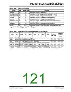
TABLE 10-9: PORTE FUNCTIONS
Name
Bit#
Buffer Type
Function
RE0/AD8/RD/P2D
bit 0
ST/TTL(1)
Input/output port pin, address/data bit 8, read control for Parallel Slave
Port or Enhanced PWM 2 output P2D
For RD (PSP Control mode):
1= Not a read operation
0= Read operation, reads PORTD register (if chip selected)
RE1/AD9/WR/P2C
RE2/AD10/CS/P2B
bit 1
bit 2
ST/TTL(1)
ST/TTL(1)
Input/output port pin, address/data bit 9, write control for Parallel Slave
Port or Enhanced PWM 2 output P2C
For WR (PSP Control mode):
1= Not a write operation
0= Write operation, writes PORTD register (if chip selected)
Input/output port pin, address/data bit 10, chip select control for
Parallel Slave Port or Enhanced PWM 2 output P2B
For CS (PSP Control mode):
1= Device is not selected
0= Device is selected
RE3/AD11/P3C(2)
RE4/AD12/P3B(2)
RE5/AD13/P1C(2)
RE6/AD14/P1B(2)
bit 3
bit 4
bit 5
bit 6
bit 7
ST/TTL(1)
ST/TTL(1)
ST/TTL(1)
ST/TTL(1)
ST/TTL(1)
Input/output port pin, address/data bit 11 or Enhanced PWM 3
output P3C.
Input/output port pin, address/data bit 12 or Enhanced PWM 3
output P3B.
Input/output port pin, address/data bit 13 or Enhanced PWM 1
output P1C.
Input/output port pin, address/data bit 14 or Enhanced PWM 1
output P1B.
RE7/AD15/
Input/output port pin, address/data bit 15, Enhanced Capture 2 input/
Compare 2 output/PWM 2 output or Enhanced PWM 2 output P2A.
ECCP2(3)/P2A(3)
Legend: ST = Schmitt Trigger input, TTL = TTL input
Note 1: Input buffers are Schmitt Triggers when in I/O or CCP/ECCP modes and TTL buffers when in System Bus
or PSP Control modes.
2: Valid for all PIC18F6525/6621 devices and PIC18F8525/8621 devices when ECCPMX is set. Alternate
assignments for P1B/P1C/P3B/P3C are RH7, RH6, RH5 and RH4, respectively.
3: Valid for all PIC18F6525/6621 devices and PIC18F8525/8621 devices in Microcontroller mode when
CCP2MX is not set. RC1 is the default assignment for ECCP2/P2A for all devices in Microcontroller mode
when CCP2MX is set; RB3 is the alternate assignment for PIC18F8525/8621 devices in operating modes
except Microcontroller mode when CCP2MX is not set.
TABLE 10-10: SUMMARY OF REGISTERS ASSOCIATED WITH PORTE
Value on
Value on:
POR, BOR
Name
Bit 7
Bit 6
Bit 5
Bit 4
Bit 3
Bit 2
Bit 1
Bit 0
all other
Resets
1111 1111
xxxx xxxx
xxxx xxxx
0-00 --00
0000 ----
1111 1111
uuuu uuuu
uuuu uuuu
0000 --00
0000 ----
TRISE
PORTE Data Direction Control Register
Read PORTE pin/Write PORTE Data Latch
Read PORTE Data Latch/Write PORTE Data Latch
PORTE
LATE
MEMCON(1) EBDIS
PSPCON(2)
IBF
—
WAIT1
WAIT0
—
—
—
—
WM1
—
WM0
—
OBF
IBOV PSPMODE
Legend: x= unknown, u= unchanged, — = unimplemented, read as ‘0’. Shaded cells are not used by PORTE.
Note 1: This register is unused on PIC18F6525/6621 devices and reads as ‘0’.
2: Enabled only in Microcontroller mode for PIC18F8525/8621 devices.
DS39612B-page 116
2005 Microchip Technology Inc.

 MICROCHIP [ MICROCHIP ]