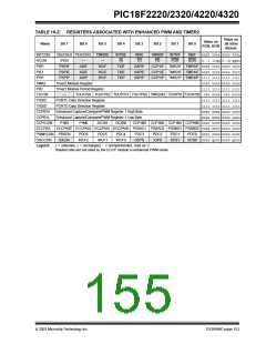
PIC18F2220/2320/4220/4320
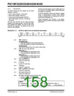
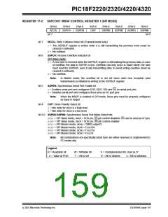
REGISTER 17-2: SSPCON1: MSSP CONTROL REGISTER 1 (SPI MODE)
R/W-0
WCOL
R/W-0
R/W-0
R/W-0
CKP
R/W-0
R/W-0
R/W-0
R/W-0
SSPOV
SSPEN
SSPM3
SSPM2
SSPM1
SSPM0
bit 7
bit 0
bit 7
bit 6
WCOL: Write Collision Detect bit (Transmit mode only)
1= The SSPBUF register is written while it is still transmitting the previous word (must be
cleared in software)
0= No collision
SSPOV: Receive Overflow Indicator bit
SPI Slave mode:
1= A new byte is received while the SSPBUF register is still holding the previous data. In case
of overflow, the data in SSPSR is lost. Overflow can only occur in Slave mode.The user
must read the SSPBUF, even if only transmitting data, to avoid setting overflow (must be
cleared in software).
0= No overflow
Note:
In Master mode, the overflow bit is not set since each new reception (and
transmission) is initiated by writing to the SSPBUF register.
bit 5
bit 4
SSPEN: Synchronous Serial Port Enable bit
1= Enables serial port and configures SCK, SDO, SDI and SS as serial port pins
0= Disables serial port and configures these pins as I/O port pins
Note:
When the MSSP is enabled in SPI mode, these pins must be properly configured
as input or output.
CKP: Clock Polarity Select bit
1= Idle state for clock is a high level
0= Idle state for clock is a low level
bit 3-0 SSPM3:SSPM0: Synchronous Serial Port Mode Select bits
0101= SPI Slave mode, clock = SCK pin, SS pin control disabled, SS can be used as I/O pin
0100= SPI Slave mode, clock = SCK pin, SS pin control enabled
0011= SPI Master mode, clock = TMR2 output/2
0010= SPI Master mode, clock = FOSC/64
0001= SPI Master mode, clock = FOSC/16
0000= SPI Master mode, clock = FOSC/4
Note:
Bit combinations not specifically listed here are either reserved or implemented in
I2C mode only.
Legend:
R = Readable bit
W = Writable bit
‘1’ = Bit is set
U = Unimplemented bit, read as ‘0’
‘0’ = Bit is cleared x = Bit is unknown
- n = Value at POR
2003 Microchip Technology Inc.
DS39599C-page 157

 MICROCHIP [ MICROCHIP ]