PIC18F2220/2320/4220/4320
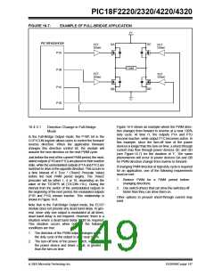
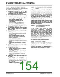
FIGURE 16-8:
PWM DIRECTION CHANGE
(1)
Period
Period
SIGNAL
P1A (Active High)
P1B (Active High)
DC
P1C (Active High)
P1D (Active High)
(Note 2)
DC
Note 1: The direction bit in the CCP1 Control register (CCP1CON<7>) is written any time during the PWM cycle.
2: When changing directions, the P1A and P1C signals switch before the end of the current PWM cycle at intervals of
4 TOSC, 16 TOSC or 64 TOSC, depending on the Timer2 prescaler value. The modulated P1B and P1D signals are
inactive at this time.
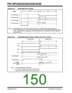
FIGURE 16-9:
PWM DIRECTION CHANGE AT NEAR 100% DUTY CYCLE(1)
Forward Period
Reverse Period
t1
P1A
P1B
DC
P1C
P1D
DC
(2)
t
on
External Switch C
External Switch D
(3)
t
off
(2,3)
Potential
Shoot-Through
Current
t = t – t
off
on
Note 1: All signals are shown as active-high.
2: t is the turn-on delay of power switch QC and its driver.
on
3: t is the turn-off delay of power switch QD and its driver.
off
DS39599C-page 148
2003 Microchip Technology Inc.

 MICROCHIP [ MICROCHIP ]