PIC18F2220/2320/4220/4320
FIGURE 16-7:
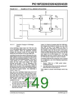
EXAMPLE OF FULL-BRIDGE APPLICATION
V+
PIC18F4220/4320
QC
QA
FET
Driver
FET
Driver
P1A
Load
P1B
FET
Driver
FET
Driver
P1C
P1D
QD
QB
V-
Figure 16-9 shows an example where the PWM direc-
tion changes from forward to reverse at a near 100%
duty cycle. At time t1, the outputs P1A and P1D
become inactive, while output P1C becomes active. In
this example, since the turn-off time of the power
devices is longer than the turn-on time, a shoot-through
current may flow through power devices QC and QD
(see Figure 16-7) for the duration of ‘t’. The same
phenomenon will occur to power devices QA and QB
for PWM direction change from reverse to forward.
16.4.3.1
Direction Change in Full-Bridge
Mode
In the Full-Bridge Output mode, the P1M1 bit in the
CCP1CON register allows users to control the forward/
reverse direction. When the application firmware
changes this direction control bit, the module will
assume the new direction on the next PWM cycle.
Just before the end of the current PWM period, the mod-
ulated outputs (P1B and P1D) are placed in their inactive
state, while the unmodulated outputs (P1A and P1C) are
switched to drive in the opposite direction. This occurs in
a time interval of 4 TOSC * (Timer2 Prescale Value)
before the next PWM period begins. The Timer2
prescaler will be either 1, 4 or 16, depending on the
value of the T2CKPS bit (T2CON<1:0>). During the
interval from the switch of the unmodulated outputs to
the beginning of the next period, the modulated outputs
(P1B and P1D) remain inactive. This relationship is
shown in Figure 16-8.
If changing PWM direction at high duty cycle is required
for an application, one of the following requirements
must be met:
1. Reduce PWM for
changing directions.
a PWM period before
2. Use switch drivers that can drive the switches off
faster than they can drive them on.
Other options to prevent shoot-through current may
exist.
Note that in the Full-Bridge Output mode, the ECCP
module does not provide any dead band delay. In gen-
eral, since only one output is modulated at all times,
dead band delay is not required. However, there is a
situation where a dead band delay might be required.
This situation occurs when both of the following
conditions are true:
1. The direction of the PWM output changes when
the duty cycle of the output is at or near 100%.
2. The turn-off time of the power switch, including
the power device and driver circuit, is greater
than the turn-on time.
2003 Microchip Technology Inc.
DS39599C-page 147

 MICROCHIP [ MICROCHIP ]