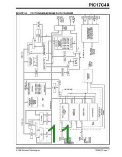
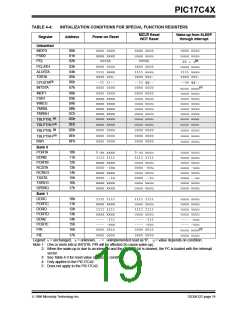
PIC17C4X
4.1
Power-on Reset (POR), Power-up
Timer (PWRT), and Oscillator Start-up
Timer (OST)
4.0
RESET
The PIC17CXX differentiates between various kinds of
reset:
• Power-on Reset (POR)
4.1.1
POWER-ON RESET (POR)
• MCLR reset during normal operation
• WDT Reset (normal operation)
The Power-on Reset circuit holds the device in reset
until VDD is above the trip point (in the range of 1.4V -
2.3V). The PIC17C42 does not produce an internal
reset when VDD declines. All other devices will produce
an internal reset for both rising and falling VDD. To take
advantage of the POR, just tie the MCLR/VPP pin
directly (or through a resistor) to VDD.This will eliminate
external RC components usually needed to create
Power-on Reset. A minimum rise time for VDD is
required. See Electrical Specifications for details.
Some registers are not affected in any reset condition;
their status is unknown on POR and unchanged in any
other reset. Most other registers are forced to a “reset
state” on Power-on Reset (POR), on MCLR or WDT
Reset and on MCLR reset during SLEEP. They are not
affected by a WDT Reset during SLEEP, since this reset
is viewed as the resumption of normal operation. The
TO and PD bits are set or cleared differently in different
reset situations as indicated in Table 4-3.These bits are
used in software to determine the nature of reset. See
Table 4-4 for a full description of reset states of all reg-
isters.
4.1.2
POWER-UP TIMER (PWRT)
The Power-up Timer provides a fixed 96 ms time-out
(nominal) on power-up. This occurs from rising edge of
the POR signal and after the first rising edge of MCLR
(detected high). The Power-up Timer operates on an
internal RC oscillator. The chip is kept in RESET as
long as the PWRT is active. In most cases the PWRT
delay allows the VDD to rise to an acceptable level.
Note: While the device is in a reset state, the
internal phase clock is held in the Q1 state.
Any processor mode that allows external
execution will force the RE0/ALE pin as a
low output and the RE1/OE and RE2/WR
pins as high outputs.
The power-up time delay will vary from chip to chip and
to VDD and temperature. See DC parameters for
details.
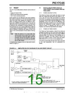
A simplified block diagram of the on-chip reset circuit is
shown in Figure 4-1.
FIGURE 4-1: SIMPLIFIED BLOCK DIAGRAM OF ON-CHIP RESET CIRCUIT
External
Reset
MCLR
WDT
Module
WDT
Time_Out
Reset
VDD rise
detect
S
R
Power_On_Reset
VDD
OST/PWRT
Chip_Reset
Q
OST
10-bit Ripple counter
OSC1
PWRT
On-chip
RC OSC†
10-bit Ripple counter
Power_Up
(Enable the PWRT timer
only during Power_Up)
(Power_Up + Wake_Up) (XT + LF)
(Enable the OST if it is Power_Up or Wake_Up
from SLEEP and OSC type is XT or LF)
† This RC oscillator is shared with the WDT
when not in a power-up sequence.
1996 Microchip Technology Inc.
DS30412C-page 15
This document was created with FrameMaker 4 0 4

 MICROCHIP [ MICROCHIP ]