PIC17C4X
Applicable Devices 42 R42 42A 43 R43 44
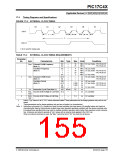
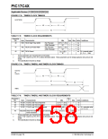
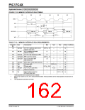
FIGURE 17-5: TIMER0 CLOCK TIMINGS
RA1/T0CKI
40
41
42
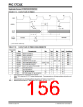
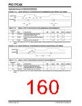
TABLE 17-5: TIMER0 CLOCK REQUIREMENTS
Parameter
No.
Sym Characteristic
Min
Typ† Max Units Conditions
40
Tt0H T0CKI High Pulse Width
No Prescaler
With Prescaler
No Prescaler
With Prescaler
0.5TCY + 20 §
10*
—
—
—
—
—
—
—
—
—
—
ns
ns
ns
ns
41
42
Tt0L T0CKI Low Pulse Width
Tt0P T0CKI Period
0.5TCY + 20 §
10*
TCY + 40 §
N
ns N = prescale value
(1, 2, 4, ..., 256)
*
These parameters are characterized but not tested.
†
Data in "Typ" column is at 5V, 25˚C unless otherwise stated. These parameters are for design guidance only and are not
tested.
§
This specification ensured by design.
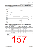
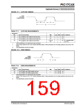
FIGURE 17-6: TIMER1,TIMER2, AND TIMER3 CLOCK TIMINGS
TCLK12
or
TCLK3
46
45
47
48
48
TMRx
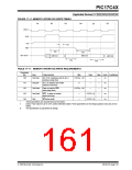
TABLE 17-6: TIMER1,TIMER2, AND TIMER3 CLOCK REQUIREMENTS
Parameter
No.
Typ
†
Sym
Characteristic
Min
Max Units Conditions
45
46
47
Tt123H TCLK12 and TCLK3 high time
Tt123L TCLK12 and TCLK3 low time
Tt123P TCLK12 and TCLK3 input period
0.5 TCY + 20 §
0.5 TCY + 20 §
—
—
—
—
—
—
ns
ns
TCY + 40 §
N
ns N = prescale value
(1, 2, 4, 8)
48
TckE2tmrI Delay from selected External Clock Edge to
Timer increment
2TOSC §
—
6 Tosc §
—
*
These parameters are characterized but not tested.
†
Data in "Typ" column is at 5V, 25˚C unless otherwise stated. These parameters are for design guidance only and are not
tested.
§
This specification ensured by design.
DS30412C-page 158
1996 Microchip Technology Inc.

 MICROCHIP [ MICROCHIP ]