PIC17C4X
Applicable Devices 42 R42 42A 43 R43 44
17.4
Timing Diagrams and Specifications
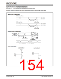
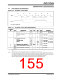
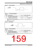
FIGURE 17-2: EXTERNAL CLOCK TIMING
Q4
Q3
Q4
Q1
Q1
Q2
OSC1
1
3
3
4
4
2
OSC2 †
† In EC and RC modes only.
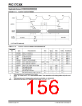
TABLE 17-2: EXTERNAL CLOCK TIMING REQUIREMENTS
Parameter
No.
Sym
Characteristic
Min Typ†
Max
Units
Conditions
DC
DC
—
—
16
25
MHz EC osc mode - PIC17C42-16
Fosc External CLKIN Frequency
MHz
- PIC17C42-25
(Note 1)
Oscillator Frequency
(Note 1)
DC
1
1
—
—
—
—
4
16
25
2
MHz RC osc mode
MHz XT osc mode - PIC17C42-16
MHz
- PIC17C42-25
DC
MHz LF osc mode
1
Tosc External CLKIN Period
62.5
40
—
—
—
—
ns
ns
EC osc mode - PIC17C42-16
- PIC17C42-25
(Note 1)
Oscillator Period
(Note 1)
250
62.5
40
—
—
—
—
—
ns
ns
ns
ns
RC osc mode
XT osc mode - PIC17C42-16
- PIC17C42-25
1,000
1,000
—
500
LF osc mode
2
3
TCY
Instruction Cycle Time (Note 1)
160
4/Fosc
—
DC
—
ns
ns
TosL, Clock in (OSC1) High or Low Time 10 ‡
TosH
EC oscillator
EC oscillator
4
TosR, Clock in (OSC1) Rise or Fall Time
—
—
5 ‡
ns
TosF
†
‡
Data in “Typ” column is at 5V, 25˚C unless otherwise stated. These parameters are for design guidance only and are not
tested.
These parameters are for design guidance only and are not tested, nor characterized.
Note 1: Instruction cycle period (TCY) equals four times the input oscillator time-base period. All specified values are based on
characterization data for that particular oscillator type under standard operating conditions with the device executing code.
Exceeding these specified limits may result in unstable oscillator operation and/or higher than expected current consump-
tion. All devices are tested to operate at “min.” values with an external clock applied to the OSC1 pin.
When an external clock input is used, the “Max.” cycle time limit is “DC” (no clock) for all devices.
1996 Microchip Technology Inc.
DS30412C-page 155

 MICROCHIP [ MICROCHIP ]