PIC17C4X
Applicable Devices 42 R42 42A 43 R43 44
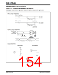
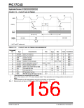
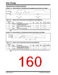
FIGURE 17-3: CLKOUT AND I/O TIMING
Q1
Q2
Q3
Q4
OSC1
11
10
22
23
OSC2 †
12
13
14
16
I/O Pin
(input)
15
17
I/O Pin
(output)
new value
old value
20, 21
† In EC and RC modes only.
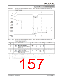
TABLE 17-3: CLKOUT AND I/O TIMING REQUIREMENTS
Parameter
No.
Sym
Characteristic
Min
Typ†
Max
Units Conditions
10
11
12
13
14
15
16
17
20
21
22
23
TosH2ckL
OSC1↑ to CLKOUT↓
—
15 ‡
15 ‡
5 ‡
5 ‡
—
30 ‡
30 ‡
15 ‡
15 ‡
ns
ns
ns
ns
ns
ns
ns
ns
ns
ns
ns
ns
Note 1
Note 1
Note 1
Note 1
Note 1
Note 1
Note 1
TosH2ckH OSC1↑ to CLKOUT↑
—
TckR
CLKOUT rise time
—
TckF
CLKOUT fall time
—
TckH2ioV
TioV2ckH
TckH2ioI
TosH2ioV
TioR
CLKOUT↑ to Port out valid
Port in valid before CLKOUT↑
Port in hold after CLKOUT↑
OSC1↑ (Q1 cycle) to Port out valid
Port output rise time
—
0.5TCY + 20‡
0.25TCY + 25 ‡
—
—
—
0 ‡
—
—
—
100 ‡
35 ‡
35 ‡
—
—
10 ‡
10 ‡
—
TioF
Port output fall time
—
TinHL
INT pin high or low time
RB7:RB0 change INT high or low time
25 *
25 *
TrbHL
—
—
*
These parameters are characterized but not tested.
†
Data in "Typ" column is at 5V, 25˚C unless otherwise stated. These parameters are for design guidance only and are not
tested.
‡
These parameters are for design guidance only and are not tested, nor characterized.
Note 1: Measurements are taken in EC Mode where OSC2 output = 4 x TOSC = TCY.
DS30412C-page 156
1996 Microchip Technology Inc.

 MICROCHIP [ MICROCHIP ]