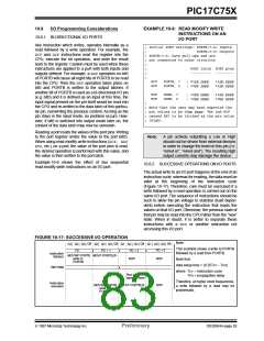
PIC17C75X
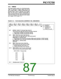
12.0 TIMER0
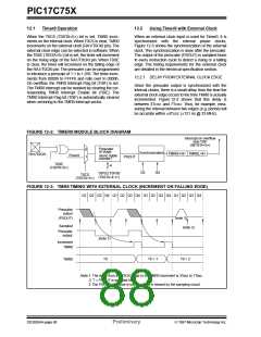
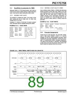
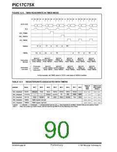
The Timer0 module consists of a 16-bit timer/counter,
TMR0. The high byte is register TMR0H and the low
byte is register TMR0L. A software programmable 8-bit
prescaler makes Timer0 an effective 24-bit overflow
timer. The clock source is software programmable as
either the internal instruction clock or an external clock
on the RA1/T0CKI pin. The control bits for this module
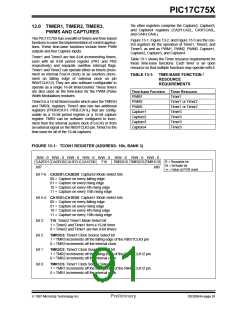
are in register T0STA (Figure 12-1).
FIGURE 12-1: T0STA REGISTER (ADDRESS: 05h, UNBANKED)
R/W - 0 R/W - 0 R/W - 0 R/W - 0 R/W - 0 R/W - 0 R/W - 0
U - 0
R = Readable bit
W = Writable bit
U = Unimplemented,
Read as '0'
INTEDG
T0SE
T0CS
T0PS3
T0PS2
T0PS1
T0PS0
—
bit7
bit0
-n = Value at POR reset
bit 7:
bit 6:
INTEDG: RA0/INT Pin Interrupt Edge Select bit
This bit selects the edge upon which the interrupt is detected
1 = Rising edge of RA0/INT pin generates interrupt
0 = Falling edge of RA0/INT pin generates interrupt
T0SE: Timer0 Clock Input Edge Select bit
This bit selects the edge upon which TMR0 will increment
When T0CS = 0 (External Clock)
1 = Rising edge of RA1/T0CKI pin increments TMR0 and/or generates a T0CKIF interrupt
0 = Falling edge of RA1/T0CKI pin increments TMR0 and/or generates a T0CKIF interrupt
When T0CS = 1 (Internal Clock)
Don’t care
bit 5:
T0CS: Timer0 Clock Source Select bit
This bit selects the clock source for TMR0.
1 = Internal instruction clock cycle (TCY)
0 = External Clock input on the T0CKI pin
bit 4-1: T0PS3:T0PS0: Timer0 Prescale Selection bits
These bits select the prescale value for TMR0.
T0PS3:T0PS0 Prescale Value
0000
0001
0010
0011
0100
0101
0110
0111
1xxx
1:1
1:2
1:4
1:8
1:16
1:32
1:64
1:128
1:256
bit 0:
Unimplemented: Read as '0'
1997 Microchip Technology Inc.
Preliminary
DS30264A-page 87

 MICROCHIP [ MICROCHIP ]