PIC17C75X
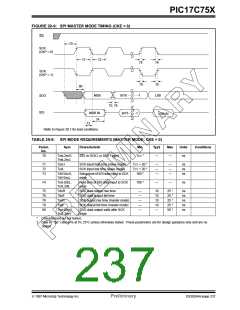
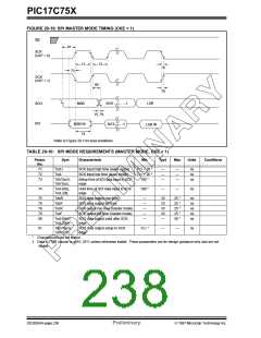
FIGURE 20-10: SPI MASTER MODE TIMING (CKE = 1)
SS
81
SCK
(CKP = 0)
71
72
79
78
73
SCK
(CKP = 1)
80
LSB
MSB
BIT6 - - - - - -1
BIT6 - - - -1
SDO
SDI
75, 76
MSB IN
74
LSB IN
Refer to Figure 20-1 for load conditions.
TABLE 20-10: SPI MODE REQUIREMENTS (MASTER MODE, CKE = 1)
Param.
No.
Sym
Characteristic
Min
Typ†
Max
Units
Conditions
71
72
73
TscH
SCK input high time (slave mode)
SCK input low time (slave mode)
TCY + 20 *
TCY + 20 *
100 *
—
—
—
—
—
—
ns
ns
ns
TscL
TdiV2scH,
TdiV2scL
Setup time of SDI data input to SCK
edge
74
TscH2diL,
TscL2diL
Hold time of SDI data input to SCK
edge
100 *
—
—
ns
75
76
78
79
80
TdoR
TdoF
TscR
TscF
SDO data output rise time
—
—
—
—
—
10
10
10
10
—
25 *
25 *
25 *
25 *
50 *
ns
ns
ns
ns
ns
SDO data output fall time
SCK output rise time (master mode)
SCK output fall time (master mode)
TscH2doV,
TscL2doV
SDO data output valid after SCK
edge
81
TdoV2scH,
TdoV2scL
SDO data output setup to SCK
edge
TCY *
—
—
ns
*
Characterized but not tested.
†
Data in "Typ" column is at 5V, 25˚C unless otherwise stated. These parameters are for design guidance only and are not
tested.
DS30264A-page 238
Preliminary
1997 Microchip Technology Inc.

 MICROCHIP [ MICROCHIP ]