PIC17C75X
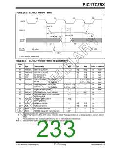
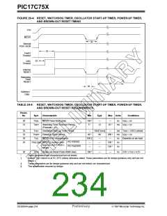
FIGURE 20-4: RESET, WATCHDOG TIMER, OSCILLATOR START-UP TIMER, POWER-UP TIMER,
AND BROWN-OUT RESET TIMING
VDD
MCLR
30
Internal
POR / BOR
33
PWRT
Timeout
32
OSC
Timeout
Internal
RESET
Watchdog
Timer
RESET
31
35
Address /
Data
TABLE 20-4: RESET, WATCHDOG TIMER, OSCILLATOR START-UP TIMER, POWER-UP TIMER,
AND BROWN-OUT RESET REQUIREMENTS
Param.
No.
Sym
Characteristic
Min
Typ†
Max Units
Conditions
30
31
TmcL
TWDT
MCLR Pulse Width (low)
100 *
5 *
—
—
ns
VDD = 5V
VDD = 5V
Watchdog Timer Time-out Period
(Prescale = 1)
12
25 *
ms
32
33
34
TOST
TPWRT
TIOZ
Oscillation Start-up Timer Period
Power-up Timer Period
—
1024TOSC§
—
200 *
—
ms TOSC = OSC1 period
ms
40 *
96
—
VDD = 5V
MCLR to I/O hi-impedance
100 ‡
ns Depends on pin load
PIC17CXXX
35
TmcL2adI MCLR to System Inter-
face bus (AD15:AD0>)
invalid
—
—
—
—
100 *
120 *
ns
ns
PIC17LCXXX
36
TBOR
Brown-out Reset Pulse Width (low)
100 *
—
—
ns 3.8V ≤ VDD ≤ 4.2V
*
These parameters are characterized but not tested.
†
Data in “Typ” column is at 5V, 25°C unless otherwise stated. These parameters are for design guidance only and are not
tested.
‡
§
These parameters are for design guidance only and are not tested, nor characterized.
This specification ensured by design.
DS30264A-page 234
Preliminary
1997 Microchip Technology Inc.

 MICROCHIP [ MICROCHIP ]