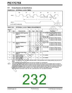
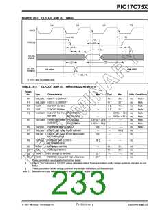
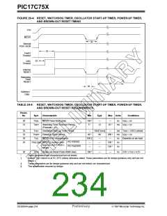
PIC17C75X
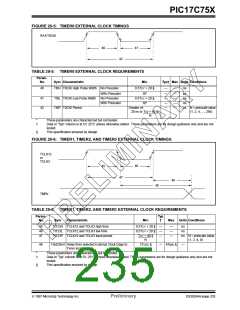
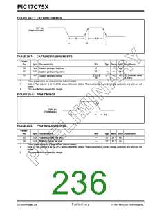
FIGURE 20-7: CAPTURE TIMINGS
CAP pin
(Capture Mode)
50
51
52
TABLE 20-7: CAPTURE REQUIREMENTS
Param.
No.
Sym Characteristic
Min
Typ† Max Units Conditions
50
51
TccL Capture pin input low time
10 *
10 *
—
—
—
—
ns
ns
TccH
TccP
Capture pin input high time
Capture pin input period
52
2TCY §
N
—
—
ns N = prescale value
(4 or 16)
*
These parameters are characterized but not tested.
†
Data in “Typ” column is at 5V, 25°C unless otherwise stated. These parameters are for design guidance only and are not
tested.
§
This specification ensured by design.
FIGURE 20-8: PWM TIMINGS
PWM pin
(PWM Mode)
53
54
TABLE 20-8: PWM REQUIREMENTS
Param.
No.
Sym Characteristic
Min
Typ† Max Units Conditions
53
54
TccR PWM pin output rise time
TccF PWM pin output fall time
—
—
10 * 35 *
10 * 35 *
ns
ns
*
These parameters are characterized but not tested.
†
Data in “Typ” column is at 5V, 25°C unless otherwise stated. These parameters are for design guidance only and are not
tested.
§
This specification ensured by design.
DS30264A-page 236
Preliminary
1997 Microchip Technology Inc.

 MICROCHIP [ MICROCHIP ]