PIC17C75X
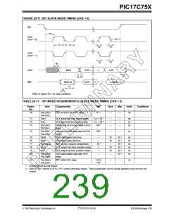
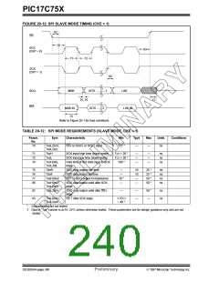
FIGURE 20-12: SPI SLAVE MODE TIMING (CKE = 1)
82
SS
70
SCK
83
(CKP = 0)
71
72
SCK
(CKP = 1)
80
MSB
BIT6 - - - - - -1
BIT6 - - - -1
LSB
SDO
SDI
75, 76
77
MSB IN
74
LSB IN
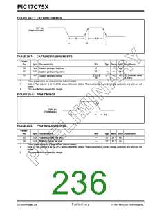
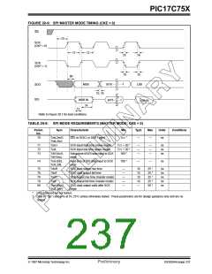
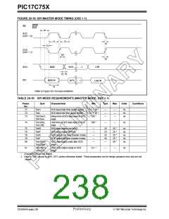
Refer to Figure 20-1 for load conditions.
TABLE 20-12: SPI MODE REQUIREMENTS (SLAVE MODE, CKE = 1)
Param.
No.
Sym
Characteristic
Min
Typ†
Max
Units
Conditions
70
TssL2scH,
TssL2scL
SS↓ to SCK↓ or SCK↑ input
TCY *
—
—
ns
71
72
74
TscH
TscL
SCK input high time (slave mode)
SCK input low time (slave mode)
TCY + 20 *
TCY + 20 *
100 *
—
—
—
—
—
—
ns
ns
ns
TscH2diL,
TscL2diL
Hold time of SDI data input to SCK
edge
75
76
77
80
TdoR
SDO data output rise time
SDO data output fall time
—
—
10
10
—
—
25 *
25 *
50 *
50 *
ns
ns
ns
ns
TdoF
TssH2doZ
SS↑ to SDO output hi-impedance
10 *
—
TscH2doV,
TscL2doV
SDO data output valid after SCK
edge
82
83
TssL2doV
SDO data output valid after SS↓
edge
—
—
—
50 *
—
ns
ns
TscH2ssH,
TscL2ssH
SS ↑ after SCK edge
1.5TCY
+ 40 *
*
Characterized but not tested.
†
Data in "Typ" column is at 5V, 25˚C unless otherwise stated. These parameters are for design guidance only and are not
tested.
DS30264A-page 240
Preliminary
1997 Microchip Technology Inc.

 MICROCHIP [ MICROCHIP ]