PIC17C75X
5.0
RESET
Note: While the device is in a reset state, the
internal phase clock is held in the Q1 state.
Any processor mode that allows external
execution will force the RE0/ALE pin as a
low output and the RE1/OE and RE2/WR
pins as high outputs.
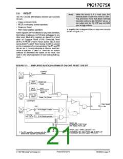
The PIC17CXXX differentiates between various kinds
of reset:
• Power-on Reset (POR)
• MCLR reset during normal operation
• Brown-out Reset
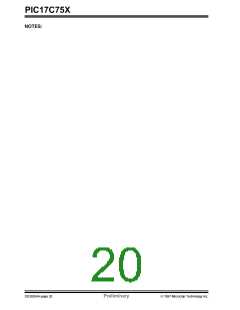
A simplified block diagram of the on-chip reset circuit is
shown in Figure 5-1.
• WDT Reset (normal operation)
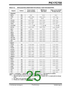
Some registers are not affected in any reset condition,
their status is unknown on POR and unchanged in any
other reset. Most other registers are forced to a “reset
state” on Power-on Reset (POR), Brown-out Reset
(BOR), on MCLR or WDT Reset and on MCLR reset
during SLEEP. A WDT Reset during SLEEP, is viewed
as the resumption of normal operation.The TO and PD
bits are set or cleared differently in different reset situ-
ations as indicated in Table 5-3. These bits are used in
software to determine the nature of the reset. See
Table 5-4 for a full description of reset states of all reg-
isters.
FIGURE 5-1: SIMPLIFIED BLOCK DIAGRAM OF ON-CHIP RESET CIRCUIT
External
Reset
MCLR
BOR
Module
Brown-out
Reset
WDT
Module
WDT
Time_Out
Reset
VDD rise
detect
S
R
Power_On_Reset
VDD
OST/PWRT
Chip_Reset
Q
OST
10-bit Ripple counter
OSC1
PWRT
On-chip
RC OSC†
10-bit Ripple counter
Power_Up
(Enable the PWRT timer
only during Power_Up)
(Power_Up) + (Wake_Up) (XT + LF)
(Enable the OST if it is Power_Up or Wake_Up
† This RC oscillator is shared with the WDT
when not in a power-up sequence.
from SLEEP and OSC type is XT or LF)
1997 Microchip Technology Inc.
Preliminary
DS30264A-page 21

 MICROCHIP [ MICROCHIP ]