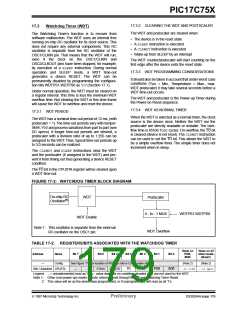
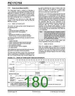
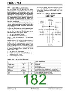
PIC17C75X
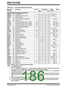
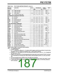
TABLE 18-1: OPCODE FIELD
18.0 INSTRUCTION SET SUMMARY
DESCRIPTIONS
The PIC17CXXX instruction set consists of 58 instruc-
tions. Each instruction is a 16-bit word divided into an
OPCODE and one or more operands. The opcode
specifies the instruction type, while the operand(s) fur-
ther specify the operation of the instruction. The
PIC17CXXX instruction set can be grouped into three
types:
Field
Description
f
p
i
Register file address (00h to FFh)
Peripheral register file address (00h to 1Fh)
Table pointer control i = '0' (do not change)
i = '1' (increment after instruction execution)
t
Table byte select t = '0' (perform operation on lower
byte)
t = '1' (perform operation on upper byte literal field,
constant data)
• byte-oriented
• bit-oriented
• literal and control operations.
These formats are shown in Figure 18-1.
WREG Working register (accumulator)
b
k
x
Bit address within an 8-bit file register
Literal field, constant data or label
Table 18-1 shows the field descriptions for the
opcodes. These descriptions are useful for under-
standing the opcodes in Table 18-2 and in each specific
instruction descriptions.
Don't care location (= '0' or '1')
The assembler will generate code with x = '0'. It is
the recommended form of use for compatibility with
all Microchip software tools.
byte-oriented instructions, 'f' represents a file regis-
ter designator and 'd' represents a destination designa-
tor. The file register designator specifies which file
register is to be used by the instruction.
d
Destination select
0 = store result in WREG
1 = store result in file register f
Default is d = '1'
The destination designator specifies where the result of
the operation is to be placed. If 'd' = '0', the result is
placed in the WREG register. If 'd' = '1', the result is
placed in the file register specified by the instruction.
u
s
Unused, encoded as '0'
Destination select
0 = store result in file register f and in the WREG
1 = store result in file register f
Default is s = '1'
bit-oriented instructions, 'b' represents a bit field des-
ignator which selects the number of the bit affected by
the operation, while 'f' represents the number of the file
in which the bit is located.
label Label name
C,DC, ALU status bits Carry, Digit Carry, Zero, Overflow
Z,OV
literal and control operations, 'k' represents an 8- or
13-bit constant or literal value.
GLINTD Global Interrupt Disable bit (CPUSTA<4>)
TBLPTR Table Pointer (16-bit)
The instruction set is highly orthogonal and is grouped
into:
TBLAT Table Latch (16-bit) consists of high byte (TBLATH)
and low byte (TBLATL)
• byte-oriented operations
• bit-oriented operations
• literal and control operations
TBLATL Table Latch low byte
TBLATH Table Latch high byte
TOS Top of Stack
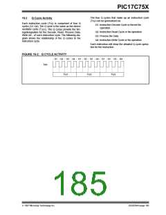
All instructions are executed within one single instruc-
tion cycle, unless:
PC
Program Counter
BSR Bank Select Register
• a conditional test is true
• the program counter is changed as a result of an
instruction
• a table read or a table write instruction is exe-
cuted (in this case, the execution takes two
instruction cycles with the second cycle executed
as a NOP)
WDT Watchdog Timer Counter
TO
PD
Time-out bit
Power-down bit
dest Destination either the WREG register or the speci-
fied register file location
[ ]
( )
→
Options
Contents
One instruction cycle consists of four oscillator periods.
Thus, for an oscillator frequency of 25 MHz, the normal
instruction execution time is 160 ns. If a conditional test
is true or the program counter is changed as a result of
an instruction, the instruction execution time is 320 ns.
Assigned to
Register bit field
In the set of
< >
User defined term (font is courier)
italics
1997 Microchip Technology Inc.
DS30264A-page 183

 MICROCHIP [ MICROCHIP ]