PIC17C75X
For complete details of serial programming, please
refer to the PIC17C75X Programming Specification.
(Contact your local Microchip Technology Sales Office
for availability.)
17.6
In-Circuit Serial Programming
The PIC17C75X group of the high end family
(PIC17CXXX) has an added feature that allows serial
programming while in the end application circuit.This is
simply done with two lines for clock and data, and three
other lines for power, ground, and the programming
voltage. This allows customers to manufacture boards
with unprogrammed devices, and then program the
microcontroller just before shipping the product. This
also allows the most recent firmware or a custom firm-
ware to be programmed.
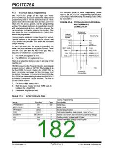
FIGURE 17-4: TYPICAL IN-CIRCUIT SERIAL
PROGRAMMING
CONNECTION
To Normal
Connections
External
Connector
Signals
PIC17C75X
Devices may be serialized to make the product unique,
“special” variants of the product may be offered, and
code updates are possible. This allows for increased
design flexibility.
+5V
0V
VDD
VSS
VPP
MCLR/VPP
To place the device into the serial programming test
mode, two pins will need to be placed at VIHH. These
are the TEST pin and the MCLR/VPP pin. Also a
sequence of events must occur as follows:
TEST CNTL
Dev. CLK
TEST
RA1/T0CKI
Data I/O
RA4/RX1/DT1
RA5/TX1/CK1
1. The TEST pin is placed at VIHH.
Data CLK
2. The MCLR/VPP pin is placed at VIHH.
There is a setup time between step 1 and step 2 that
must be met.
After this sequence the Program Counter is pointing to
program memory address 0xFF60. This location is in
the Boot ROM. The code initializes the USART/SCI so
that it can receive commands. For this, the device must
be clocked.The device clock source in this mode is the
RA1/T0CKI pin. After delaying to allow the USART/SCI
to initialize, commands can be received. The flow is
shown in these 3 steps:
VDD
To Normal
Connections
1. The device clock source starts.
2. Wait 80 device clocks for Boot ROM code to
configure the USART/SCI.
3. Commands may now be sent.
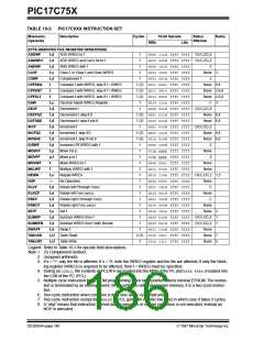
TABLE 17-3: ISP INTERFACE PINS
During Programming
Description
Name
Function
DT
Type
RA4/RX1/DT1
RA5/TX1/CK1
RA1/T0CKI
TEST
I/O
I
Serial Data
CK
Serial Clock
OSCI
TEST
MCLR/VPP
VDD
I
Device Clock Source
I
Test mode selection control input. Force to VIHH,
Master Clear reset and Device Programming Voltage
Positive supply for logic and I/O pins
MCLR/VPP
VDD
P
P
P
VSS
VSS
Ground reference for logic and I/O pins
DS30264A-page 182
Preliminary
1997 Microchip Technology Inc.

 MICROCHIP [ MICROCHIP ]