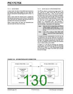
PIC17C75X
2
Two pins are used for data transfer. These are the SCL
pin, which is the clock, and the SDA pin, which is the
data. Pins that are on PortA are automatically config-
ured when the I C mode is enabled. The SSP module
functions are enabled by setting SSP Enable bit
SSPEN (SSPCON1<5>).
15.2
SSP I C Operation
2
The SSP module in I C mode fully implements all mas-
ter and slave functions (including general call support)
and provides interrupts on start and stop bits in hard-
ware to determine a free bus (multi-master function).
The SSP module implements the standard mode spec-
ifications as well as 7-bit and 10-bit addressing.
2
2
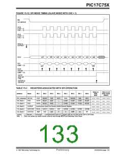
The SSP module has six registers for I C operation.
2
These are the:
Appendix E gives an overview of the I C bus specifica-
tion.
• SSP Control Register1 (SSPCON1)
• SSP Control Register2 (SSPCON2)
• SSP Status Register (SSPSTAT)
• Serial Receive/Transmit Buffer (SSPBUF)
• SSP Shift Register (SSPSR) - Not directly acces-
sible
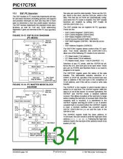
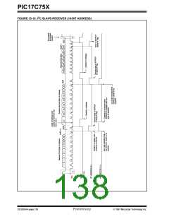
FIGURE 15-13: SSP BLOCK DIAGRAM
2
(I C MODE)
Internal
data bus
Read
Write
• SSP Address Register (SSPADD)
2
The SSPCON1 register allows control of the I C oper-
SSPBUF reg
SSPSR reg
SCL
SDA
ation. Four mode selection bits (SSPCON1<3:0>)
allow one of the following I C modes to be selected:
2
shift
clock
2
• I C Slave mode (7-bit address)
2
• I C Slave mode (10-bit address)
2
• I C Master mode, clock = OSC/4 (SSPADD +1)
MSb
LSb
2
Selection of any I C mode, with the SSPEN bit set,
forces the SCL and SDA pins to be open drain. These
pins are on PORTA and therefore there is no need to
program to be inputs.
Addr Match
Match detect
SSPADD reg
The SSPSTAT register gives the status of the data
transfer. This information includes detection of a
START or STOP bit, specifies if the received byte was
data or address if the next byte is the completion of
10-bit address, and if this will be a read or write data
transfer.
Set, Reset
S, P bits
(SSPSTAT reg)
Start and
Stop bit detect
2
FIGURE 15-14: I C MASTER MODE BLOCK
DIAGRAM
The SSPBUF is the register to which transfer data is
written to or read from. The SSPSR register shifts the
data in or out of the device. In receive operations, the
SSPBUF and SSPSR create a doubled buffered
receiver. This allows reception of the next byte to begin
before reading the last byte of received data. When the
complete byte is received, it is transferred to the
SSPBUF register and flag bit SSPIF is set. If another
complete byte is received before the SSPBUF register
is read, a receiver overflow has occurred and bit
SSPOV (SSPCON1<6>) is set and the byte in the
SSPSR is lost.
Internal
data bus
Read
Write
SSPADD<6:0>
7
Baud Rate Generator
SSPBUF reg
SSPSR reg
SCL
shift
clock
The SSPADD register holds the slave address. In
10-bit mode, the user needs to write the high byte of the
address (1111 0 A9 A8 0). Following the high byte
address match, the low byte of the address needs to be
loaded (A7:A0).
SDA
MSb
LSb
Addr Match
Match detect
SSPADD reg
Set/Clear S bit
and
Clear/Set P, bits
(SSPSTAT reg)
Start and Stop bit
detect / generate
and Set SSPIF
DS30264A-page 134
Preliminary
1997 Microchip Technology Inc.

 MICROCHIP [ MICROCHIP ]