PIC16F913/914/916/917/946
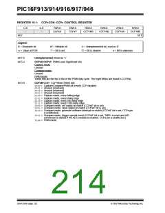
REGISTER 15-1: CCPxCON: CCPx CONTROL REGISTER
U-0
—
U-0
—
R/W-0
R/W-0
R/W-0
R/W-0
R/W-0
R/W-0
CCPxX
CCPxY
CCP1M3
CCP1M2
CCP1M1
CCP1M0
bit 7
bit 0
Legend:
R = Readable bit
-n = Value at POR
W = Writable bit
‘1’ = Bit is set
U = Unimplemented bit, read as ‘0’
‘0’ = Bit is cleared x = Bit is unknown
bit 7-6
bit 5-4
Unimplemented: Read as ‘0’
CCPxX:CCPxY: PWM Least Significant bits
Capture mode:
Unused
Compare mode:
Unused
PWM mode:
These bits are the two LSbs of the PWM duty cycle. The eight MSbs are found in CCPRxL.
bit 3-0
CCPxM<3:0>: CCP Mode Select bits
0000= Capture/Compare/PWM off (resets CCP module)
0001= Unused (reserved)
0010= Unused (reserved)
0011= Unused (reserved)
0100= Capture mode, every falling edge
0101= Capture mode, every rising edge
0110= Capture mode, every 4th rising edge
0111= Capture mode, every 16th rising edge
1000= Compare mode, set output on match (CCPxIF bit is set)
1001= Compare mode, clear output on match (CCPxIF bit is set)
1010= Compare mode, generate software interrupt on match (CCPxIF bit is set, CCPx pin
is unaffected)
1011= Compare mode, trigger special event (CCPxIF bit is set, TMR1 is reset and A/D
conversion is started if the ADC module is enabled. CCPx pin is unaffected.)
11xx= PWM mode.
DS41250F-page 212
© 2007 Microchip Technology Inc.

 MICROCHIP [ MICROCHIP ]