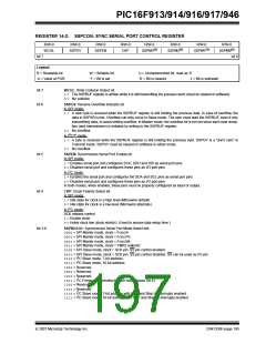
PIC16F913/914/916/917/946
even if in the middle of a transmitted byte, and becomes
a floating output. External pull-up/pull-down resistors
may be desirable, depending on the application.
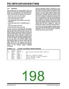
14.6 Slave Mode
In Slave mode, the data is transmitted and received as
the external clock pulses appear on SCK. When the
last bit is latched, the SSPIF interrupt flag bit is set.
Note 1: When the SPI is in Slave mode with SS
pin control enabled (SSPCON<3:0> =
0100), the SPI module will reset if the SS
pin is set to VDD.
While in Slave mode, the external clock is supplied by
the external clock source on the SCK pin. This external
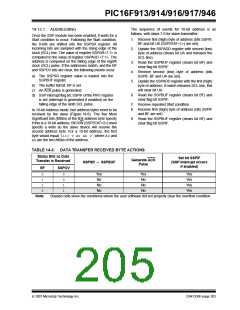
clock must meet the minimum high and low times as
specified in the electrical specifications.
2: If the SPI is used in Slave Mode with CKE
set, then the SS pin control must be
enabled.
While in Sleep mode, the slave can transmit/receive
data. When a byte is received, the device will wake-up
from Sleep.
When the SPI module resets, the bit counter is forced
to 0. This can be done by either forcing the SS pin to a
high level or clearing the SSPEN bit.
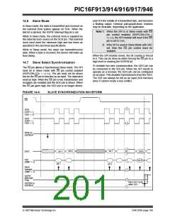
14.7 Slave Select Synchronization
To emulate two-wire communication, the SDO pin can
be connected to the SDI pin. When the SPI needs to
operate as a receiver, the SDO pin can be configured
as an input. This disables transmissions from the SDO.
The SDI can always be left as an input (SDI function)
since it cannot create a bus conflict.
The SS pin allows a Synchronous Slave mode. The SPI
must be in Slave mode with SS pin control enabled
(SSPCON<3:0> = 0100). The pin must not be driven
low for the SS pin to function as an input. The data latch
must be high. When the SS pin is low, transmission and
reception are enabled and the SDO pin is driven. When
the SS pin goes high, the SDO pin is no longer driven,
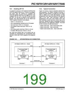
FIGURE 14-4:
SLAVE SYNCHRONIZATION WAVEFORM
SS
SCK
(CKP = 0
CKE = 0)
SCK
(CKP = 1
CKE = 0)
Write to
SSPBUF
bit 6
bit 7
bit 7
bit 0
SDO
bit 7
SDI
(SMP = 0)
bit 0
bit 7
Input
Sample
(SMP = 0)
SSPIF
Interrupt
Flag
Next Q4 Cycle
after Q2↓
SSPSR to
SSPBUF
© 2007 Microchip Technology Inc.
DS41250F-page 199

 MICROCHIP [ MICROCHIP ]