PIC16F913/914/916/917/946
14.8 Sleep Operation
14.10 Bus Mode Compatibility
In Master mode, all module clocks are halted and the
transmission/reception will remain in that state until the
device wakes from Sleep. After the device returns to
Normal mode, the module will continue to
transmit/receive data.
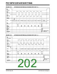
Table 14-1 shows the compatibility between the
standard SPI modes and the states of the CKP and
CKE control bits.
TABLE 14-1: SPI BUS MODES
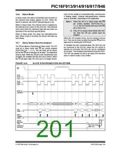
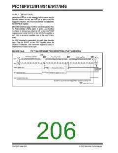
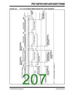
In Slave mode, the SPI Transmit/Receive Shift register
operates asynchronously to the device. This allows the
device to be placed in Sleep mode and data to be
shifted into the SPI Transmit/Receive Shift register.
When all 8 bits have been received, the SSP interrupt
flag bit will be set and if enabled, will wake the device
from Sleep.
Control Bits State
Standard SPI Mode
Terminology
CKP
CKE
0, 0
0, 1
1, 0
1, 1
0
0
1
1
1
0
1
0
14.9 Effects of a Reset
There is also a SMP bit which controls when the data is
sampled.
A Reset disables the SSP module and terminates the
current transfer.
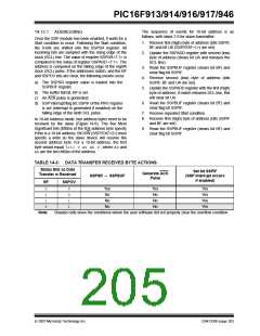
TABLE 14-2: SUMMARY OF REGISTERS ASSOCIATED WITH SPI OPERATION
Value on
POR, BOR other Resets
Value on all
Name
Bit 7
Bit 6
Bit 5
Bit 4
Bit 3
Bit 2
Bit 1
Bit 0
INTCON
LCDCON
LCDSE0
LCDSE1
PIE1
GIE
LCDEN
SE7
PEIE
SLPEN
SE6
T0IE
INTE
RBIE
CS1
T0IF
CS0
INTF
LMUX1
SE1
RBIF
0000 000x 0000 000x
WERR VLCDEN
LMUX0 0001 0011 0001 0011
SE5
SE13
RCIE
RCIF
SREN
SE4
SE12
TXIE
TXIF
SE3
SE2
SE0
SE8
0000 0000 0000 0000
0000 0000 0000 0000
0000 0000 0000 0000
0000 0000 0000 0000
SE15
EEIE
SE14
ADIE
ADIF
RX9
SE11
SE10
SE9
SSPIE
SSPIF
ADDEN
CCP1IE TMR2IE TMR1IE
CCP1IF TMR2IF TMR1IF
PIR1
EEIF
0000 000x
xxxx xxxx uuuu uuuu
SSPM0 0000 0000 0000 0000
BF 0000 0000 0000 0000
RCSTA
SPEN
CREN
FERR
OERR
RX9D
0000 000x
SSPBUF
SSPCON
SSPSTAT
TRISA
Synchronous Serial Port Receive Buffer/Transmit Register
WCOL
SMP
SSPOV
CKE
SSPEN
D/A
CKP
P
SSPM3
S
SSPM2
R/W
SSPM1
UA
TRISA7 TRISA6 TRISA5 TRISA4 TRISA3 TRISA2 TRISA1 TRISA0 1111 1111 1111 1111
TRISC7 TRISC6 TRISC5 TRISC4 TRISC3 TRISC2 TRISC1 TRISC0 1111 1111 1111 1111
x= unknown, u= unchanged, –= unimplemented, read as ‘0’. Shaded cells are not used by the SSP in SPI mode.
TRISC
Legend:
© 2007 Microchip Technology Inc.
DS41250F-page 201

 MICROCHIP [ MICROCHIP ]