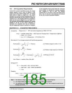
PIC16F913/914/916/917/946
13.1 EEADRL and EEADRH Registers
13.0 DATA EEPROM AND FLASH
PROGRAM MEMORY
CONTROL
The EEADRL and EEADRH registers can address up
to a maximum of 256 bytes of data EEPROM or up to a
maximum of 8K words of program Flash.
Data EEPROM memory is readable and writable and
the Flash program memory is readable during normal
operation (full VDD range). These memories are not
directly mapped in the register file space. Instead, they
are indirectly addressed through the Special Function
Registers. There are six SFRs used to access these
memories:
When selecting a program address value, the MSB of
the address is written to the EEADRH register and the
LSB is written to the EEADRL register. When selecting
a data address value, only the LSB of the address is
written to the EEADRL register.
13.1.1
EECON1 AND EECON2 REGISTERS
• EECON1
• EECON2
• EEDATL
• EEDATH
• EEADRL
• EEADRH
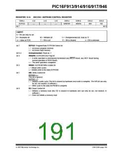
EECON1 is the control register for EE memory
accesses.
Control bit EEPGD determines if the access will be a
program or data memory access. When clear, as it is
when reset, any subsequent operations will operate on
the data memory. When set, any subsequent operations
will operate on the program memory. Program memory
can only be read.
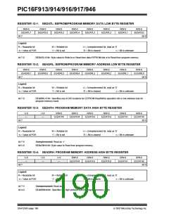
When interfacing the data memory block, EEDATL
holds the 8-bit data for read/write, and EEADRL holds
the address of the EE data location being accessed.
This device has 256 bytes of data EEPROM with an
address range from 00h to FFh.
Control bits RD and WR initiate read and write,
respectively. These bits cannot be cleared, only set, in
software. They are cleared in hardware at completion
of the read or write operation. The inability to clear the
WR bit in software prevents the accidental, premature
termination of a write operation.
When interfacing the program memory block, the
EEDATL and EEDATH registers form a 2-byte word
that holds the 14-bit data for read, and the EEADRL
and EEADRH registers form a 2-byte word that holds
the 13-bit address of the EEPROM location being
accessed. This family of devices has 4K and 8K words
of program Flash with an address range from
0h-0FFFh and 0h-1FFFh. The program memory allows
one word reads.
The WREN bit, when set, will allow a write operation to
data EEPROM. On power-up, the WREN bit is clear.
The WRERR bit is set when a write operation is inter-
rupted by a MCLR or a WDT Time-out Reset during
normal operation. In these situations, following Reset,
the user can check the WRERR bit. The Data and
Address registers will be cleared on the Reset. User
code can then run an appropriate recovery routine.
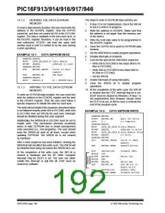
The EEPROM data memory allows byte read and write.
A byte write automatically erases the location and
writes the new data (erase before write).
Interrupt flag bit EEIF of the PIR1 register is set when
write is complete. It must be cleared in the software.
The write time is controlled by an on-chip timer. The
write/erase voltages are generated by an on-chip
charge pump rated to operate over the voltage range of
the device for byte or word operations.
EECON2 is not a physical register. Reading EECON2
will read all ‘0’s. The EECON2 register is used
exclusively in the data EEPROM write sequence.
When the device is code-protected, the CPU may
continue to read and write the data EEPROM memory
and read the program memory. When code-protected,
the device programmer can no longer access data or
program memory.
© 2007 Microchip Technology Inc.
DS41250F-page 187

 MICROCHIP [ MICROCHIP ]