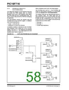
PIC16F716
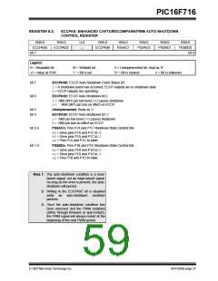
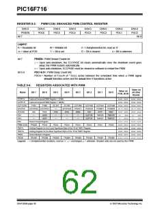
REGISTER 8-3:
PWM1CON: ENHANCED PWM CONTROL REGISTER
R/W-0
PRSEN
bit 7
R/W-0
PDC6
R/W-0
PDC5
R/W-0
PDC4
R/W-0
PDC3
R/W-0
PDC2
R/W-0
PDC1
R/W-0
PDC0
bit 0
Legend:
R = Readable bit
-n = Value at POR
W = Writable bit
‘1’ = Bit is set
U = Unimplemented bit, read as ‘0’
‘0’ = Bit is cleared x = Bit is unknown
bit 7
PRSEN: PWM Restart Enable bit
1= Upon auto-shutdown, the ECCPASE bit clears automatically once the shutdown event goes
away; the PWM restarts automatically
0= Upon auto-shutdown, ECCPASE must be cleared in software to restart the PWM
bit 6-0
PDC<6:0>: PWM Delay Count bits
PDCn = Number of FOSC/4 (4 * TOSC) cycles between the scheduled time when a PWM signal
should transition active and the actual time it transitions active
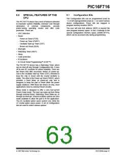
TABLE 8-6:
REGISTERS ASSOCIATED WITH PWM
Value on
Value on
POR, BOR
Name
Bit 7
Bit 6
Bit 5
Bit 4
Bit 3
Bit 2
Bit 1
Bit 0
all other
Resets
CCPR1L
CCPR1H
CCP1CON
ECCPAS
INTCON
PIE1
Capture/Compare/PWM Register 1 (LSB)
Capture/Compare/PWM Register 1 (MSB)
xxxx xxxx
xxxx xxxx
0000 0000
00-0 0000
0000 000x
-0-- -000
-0-- 0000
1111 1111
0000 0000
xxxx xxxx
xxxx xxxx
0000 0000
1111 1111
xxxx xxxx
xxxx xxxx
0000 0000
00-0 0000
0000 000x
-0-- -000
-0-- -000
1111 1111
0000 0000
xxxx xxxx
xxxx xxxx
0000 0000
1111 1111
P1M1
P1M0
DC1B1
—
DC1B0
ECCPAS0
INTE
CCP1M3
PSSAC1
RBIE
—
CCP1M2
PSSAC0
T0IF
CCP1M1
PSSBD1
INTF
CCP1M0
PSSBD0
RBIF
ECCPASE ECCPAS2
GIE
—
PEIE
ADIE
ADIF
T0IE
—
—
CCP1IE
CCP1IF
TMR2IE
TMR2IF
TMR1IE
TMR1IF
PIR1
—
—
—
—
PR2
Timer2 Period Register
PRSEN PDC6
PWM1CON
TMR1L
TMR1H
TMR2
PDC5
PDC4
PDC3
PDC2
PDC1
PDC0
Holding Register for the Least Significant Byte of the 16-bit TMR1 Register
Holding Register for the Most Significant Byte of the 16-bit TMR1 Register
Timer2 Module’s Register
TRISB
TRISB7
TRISB6
TRISB5
TRISB4
TRISB3
TRISB2
TRISB1
TRISB0
Legend: – = Unimplemented locations, read as ‘0’, u= unchanged, x= unknown. Shaded cells are not used by the PWM.
DS41206B-page 60
© 2007 Microchip Technology Inc.

 MICROCHIP [ MICROCHIP ]