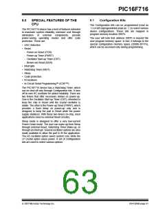
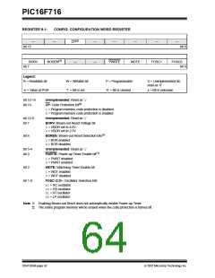
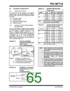
PIC16F716
8.3.10
PROGRAMMABLE DEAD-BAND
DELAY MODE
FIGURE 8-8:
EXAMPLE OF HALF-
BRIDGE PWM OUTPUT
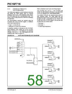
In Half-Bridge applications where all power switches
are modulated at the PWM frequency, the power
switches normally require more time to turn off than to
turn on. If both the upper and lower power switches are
switched at the same time (one turned on, and the
other turned off), both switches may be on for a short
period of time until one switch completely turns off.
During this brief interval, a very high current (shoot-
through current) will flow through both power switches,
shorting the bridge supply. To avoid this potentially
destructive shoot-through current from flowing during
switching, turning on either of the power switches is
normally delayed to allow the other switch to
completely turn off.
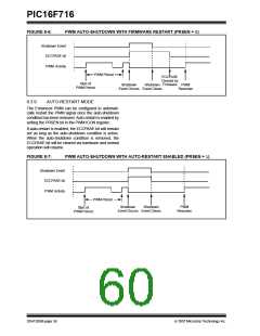
Period
Period
Pulse Width
(2)
(2)
P1A
td
td
P1B
(1)
(1)
(1)
td = Dead-Band Delay
Note 1: At this time, the TMR2 register is equal to the
PR2 register.
2: Output signals are shown as active-high.
In Half-Bridge mode, a digitally programmable dead-
band delay is available to avoid shoot-through current
from destroying the bridge power switches. The delay
occurs at the signal transition from the non-active state
to the active state. See Figure 8-8 for illustration. The
lower seven bits of the associated PWM1CON register
(Register 8-3) sets the delay period in terms of
microcontroller instruction cycles (TCY or 4 TOSC).
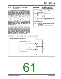
FIGURE 8-9:
EXAMPLE OF HALF-BRIDGE APPLICATIONS
V+
Standard Half-Bridge Circuit (“Push-Pull”)
FET
Driver
+
V
-
P1A
Load
FET
Driver
+
V
-
P1B
V-
© 2007 Microchip Technology Inc.
DS41206B-page 59

 MICROCHIP [ MICROCHIP ]