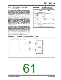
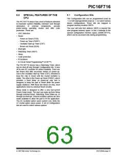
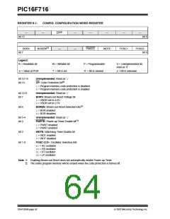
PIC16F716
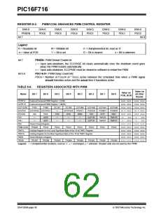
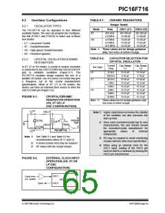
TABLE 9-1:
CERAMIC RESONATORS
Ranges Tested:
9.2
Oscillator Configurations
9.2.1
OSCILLATOR TYPES
Mode
Freq
OSC1 (C1)
OSC2 (C2)
The PIC16F716 can be operated in four different
oscillator modes. The user can program two Configura-
tion bits (FOSC1 and FOSC0) to select one of these
four modes:
XT
455 kHz
2.0 MHz
68-100 pF
15-68 pF
68-100 pF
15-68 pF
HS
4.0 MHz
8.0 MHz
16.0 MHz
10-68 pF
15-68 pF
10-22 pF
10-68 pF
15-68 pF
10-22 pF
• LP – Low-power Crystal
• XT – Crystal/Resonator
Note 1: These values are for design guidance
• HS – High-speed Crystal/Resonator
• RC – Resistor/Capacitor
only. See notes at bottom of page.
TABLE 9-2:
CAPACITOR SELECTION FOR
CRYSTAL OSCILLATOR
9.2.2
CRYSTAL OSCILLATOR/CERAMIC
RESONATORS
Crystal
Freq
Cap. Range
C1
Cap. Range
C2
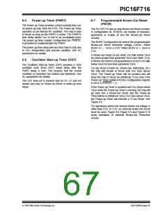
In XT, LP or HS modes, a crystal or ceramic resonator
is connected to the OSC1/CLKIN and OSC2/CLKOUT
pins to establish oscillation (Figure 9-1). The
PIC16F716 oscillator design requires the use of a
parallel cut crystal. Use of a series cut crystal may give
Osc Type
LP
32 kHz
200 kHz
200 kHz
1 MHz
15-33 pF
5-10 pF
15-33 pF
5-10 pF
XT
HS
47-68 pF
15-33 pF
15-33 pF
15-33 pF
15-33 pF
15-33 pF
47-68 pF
15-33 pF
15-33 pF
15-33 pF
15-33 pF
15-33 pF
a
frequency out of the crystal manufacturers
specifications. When in XT, LP or HS modes, the
device can have an external clock source to drive the
OSC1/CLKIN pin (Figure 9-2).
4 MHz
4 MHz
8 MHz
FIGURE 9-1:
CRYSTAL/CERAMIC
RESONATOROPERATION
(HS, XT OR LP
20 MHz
Note 1: These values are for design guidance only.
See notes at bottom of page.
OSC CONFIGURATION)
C1(1)
OSC1
Note 1: Higher capacitance increases the stability
of the oscillator, but also increases the
start-up time.
To
internal
logic
XTAL
RF(3)
2: Since each resonator/crystal has its own
characteristics, the user should consult
the resonator/crystal manufacturer for
Sleep
PIC16F716
Note 1: See Table 9-1 and Table 9-2 for
OSC2
RS(2)
C2(1)
appropriate
values
of
external
components.
3: RS may be required to avoid overdriving
recommended values of C1 and C2.
2: A series resistor (RS) may be required.
3: RF varies with the crystal chosen.
crystals with low drive level specification.
4: When using an external clock for the
OSC1 input, loading of the OSC2 pin
must be kept to a minimum by leaving the
OSC2 pin unconnected.
FIGURE 9-2:
EXTERNAL CLOCK INPUT
OPERATION (HS, XT OR
LP OSC
CONFIGURATION)
OSC1
Clock from
ext. system
PIC16F716
OSC2
Open
© 2007 Microchip Technology Inc.
DS41206B-page 63

 MICROCHIP [ MICROCHIP ]