PIC16F716
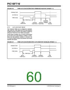
When a shutdown event occurs, two things happen:
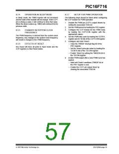
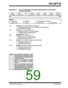
8.3.8
ENHANCED PWM AUTO-
SHUTDOWN MODE
The ECCPASE bit is set to ‘1’. The ECCPASE will
remain set until cleared in firmware or an auto-restart
occurs (see Section 8.3.9 “Auto-Restart Mode”).
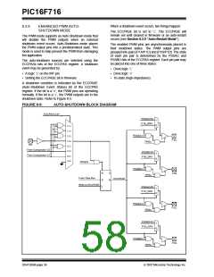
The PWM mode supports an Auto-Shutdown mode that
will disable the PWM outputs when an external
shutdown event occurs. Auto-Shutdown mode places
the PWM output pins into a predetermined state. This
mode is used to help prevent the PWM from damaging
the application.
The enabled PWM pins are asynchronously placed in
their shutdown states. The PWM output pins are
grouped into pairs [P1A/P1C] and [P1B/P1D]. The state
of each pin pair is determined by the PSSAC and
PSSBD bits of the ECCPAS register. Each pin pair may
be placed into one of three states:
The auto-shutdown sources are selected using the
ECCPASx bits of the ECCPAS register. A shutdown
event may be generated by:
• Drive logic ‘1’
• A logic ‘0’ on the INT pin
• Drive logic ‘0’
• Setting the ECCPASE bit in firmware
• Tri-state (high-impedance)
A shutdown condition is indicated by the ECCPASE
(Auto-Shutdown Event Status) bit of the ECCPAS
register. If the bit is a ‘0’, the PWM pins are operating
normally. If the bit is a ‘1’, the PWM outputs are in the
shutdown state. Refer to Figure 8-5.
FIGURE 8-5:
AUTO-SHUTDOWN BLOCK DIAGRAM
ECCPAS<2:0>
PSSAC<0>
1
P1A_DRV
0
111
110
101
100
011
010
001
000
PSSAC<1>
P1A
TRISx
INT
From Comparator C2
From Comparator C1
PSSBD<0>
1
P1B_DRV
0
PRSEN
PSSBD<1>
R
D
S
P1B
TRISx
From Data Bus
ECCPASE
Q
Write to ECCPASE
PSSAC<0>
P1C_DRV
1
0
PSSAC<1>
P1C
TRISx
PSSBD<0>
P1D_DRV
1
0
PSSBD<1>
TRISx
P1D
DS41206B-page 56
© 2007 Microchip Technology Inc.

 MICROCHIP [ MICROCHIP ]