PIC16F716
When changing the prescaler assignment from the
WDT to the Timer0 module, the following instruction
sequence must be executed (see Example 4-2).
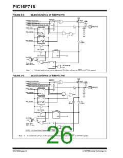
4.1.3
SOFTWARE PROGRAMMABLE
PRESCALER
A single software programmable prescaler is available
for use with either Timer0 or the Watchdog Timer
(WDT), but not both simultaneously. The prescaler
assignment is controlled by the PSA bit of the OPTION
register. To assign the prescaler to Timer0, the PSA bit
must be cleared to a ‘0’.
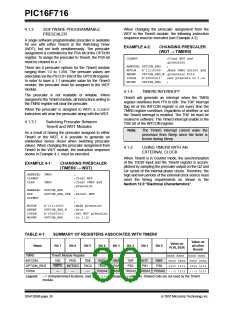
EXAMPLE 4-2:
CHANGING PRESCALER
(WDT → TIMER0)
CLRWDT
;Clear WDT and
;prescaler
;
BANKSEL OPTION_REG
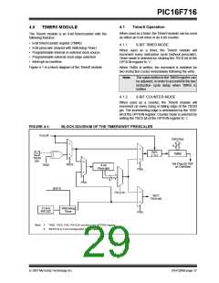
There are 8 prescaler options for the Timer0 module
ranging from 1:2 to 1:256. The prescale values are
selectable via the PS<2:0> bits of the OPTION register.
In order to have a 1:1 prescaler value for the Timer0
module, the prescaler must be assigned to the WDT
module.
MOVLW
ANDWF
IORLW
MOVWF
b’11110000’ ;Mask TMR0 select and
OPTION_REG,W ;prescaler bits
b’00000011’ ;Set prescale to 1:16
OPTION_REG
;
4.1.4
TIMER0 INTERRUPT
The prescaler is not readable or writable. When
assigned to the Timer0 module, all instructions writing to
the TMR0 register will clear the prescaler.
Timer0 will generate an interrupt when the TMR0
register overflows from FFh to 00h. The T0IF interrupt
flag bit of the INTCON register is set every time the
TMR0 register overflows, regardless of whether or not
the Timer0 interrupt is enabled. The T0IF bit must be
cleared in software. The Timer0 interrupt enable is the
T0IE bit of the INTCON register.
When the prescaler is assigned to WDT, a CLRWDT
instruction will clear the prescaler along with the WDT.
4.1.3.1
Switching Prescaler Between
Timer0 and WDT Modules
Note:
The Timer0 interrupt cannot wake the
processor from Sleep since the timer is
frozen during Sleep.
As a result of having the prescaler assigned to either
Timer0 or the WDT, it is possible to generate an
unintended device Reset when switching prescaler
values. When changing the prescaler assignment from
Timer0 to the WDT module, the instruction sequence
shown in Example 4-1, must be executed.
4.1.5
USING TIMER0 WITH AN
EXTERNAL CLOCK
When Timer0 is in Counter mode, the synchronization
of the T0CKI input and the Timer0 register is accom-
plished by sampling the prescaler output on the Q2 and
Q4 cycles of the internal phase clocks. Therefore, the
high and low periods of the external clock source must
meet the timing requirements as shown in the
Section 12.0 “Electrical Characteristics”.
EXAMPLE 4-1:
CHANGING PRESCALER
(TIMER0 → WDT)
BANKSEL TMR0
CLRWDT
;
;Clear WDT
;Clear TMR0 and
;prescaler
CLRF
TMR0
BANKSEL OPTION_REG
;
BSF
OPTION_REG,PSA ;Select WDT
CLRWDT
;
;
MOVLW
ANDWF
IORLW
MOVWF
b’11111000’
OPTION_REG,W
b’00000101’
OPTION_REG
;Mask prescaler
;bits
;Set WDT prescaler
;to 1:32
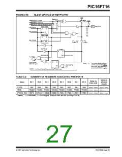
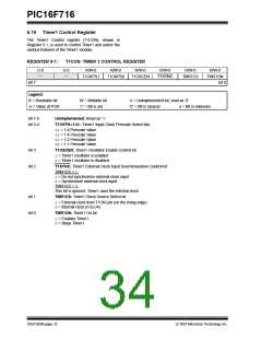
TABLE 4-1:
SUMMARY OF REGISTERS ASSOCIATED WITH TIMER0
Value on
all other
Resets
Value on
POR, BOR
Name
Bit 7
Bit 6
Bit 5
Bit 4
Bit 3
Bit 2
Bit 1
Bit 0
TMR0
Timer0 Module Register
GIE PEIE
RBPU INTEDG
xxxx xxxx uuuu uuuu
0000 000x 0000 000u
1111 1111 1111 1111
INTCON
OPTION_REG
TRISA
T0IE
T0CS
—
INTE
T0SE
RBIE
PSA
T0IF
PS2
INTF
PS1
RBIF
PS0
—
—
TRISA4 TRISA3 TRISA2 TRISA1 TRISA0 ---1 1111 ---1 1111
Legend:
– = Unimplemented locations, read as ‘0’, u= unchanged, x= unknown. Shaded cells are not used by the Timer0
module.
DS41206B-page 28
© 2007 Microchip Technology Inc.

 MICROCHIP [ MICROCHIP ]