PIC16F/LF1946/47
If the overrun occurred when the CREN bit is set then
the error condition is cleared by either clearing the
CREN bit of the RCxSTA register or by clearing the
SPEN bit which resets the EUSART.
24.4.1.6
Synchronous Master Reception
Data is received at the RXx/DTx pin. The RXx/DTx pin
output driver must be disabled by setting the
corresponding TRIS bits when the EUSART is
configured for synchronous master receive operation.
24.4.1.9
Receiving 9-bit Characters
In Synchronous mode, reception is enabled by setting
either the Single Receive Enable bit (SREN of the
RCxSTA register) or the Continuous Receive Enable
bit (CREN of the RCxSTA register).
The EUSART supports 9-bit character reception. When
the RX9 bit of the RCxSTA register is set the EUSART
will shift 9-bits into the RSR for each character
received. The RX9D bit of the RCxSTA register is the
ninth, and Most Significant, data bit of the top unread
character in the receive FIFO. When reading 9-bit data
from the receive FIFO buffer, the RX9D data bit must
be read before reading the 8 Least Significant bits from
the RCxREG.
When SREN is set and CREN is clear, only as many
clock cycles are generated as there are data bits in a
single character. The SREN bit is automatically cleared
at the completion of one character. When CREN is set,
clocks are continuously generated until CREN is
cleared. If CREN is cleared in the middle of a character
the CK clock stops immediately and the partial charac-
ter is discarded. If SREN and CREN are both set, then
SREN is cleared at the completion of the first character
and CREN takes precedence.
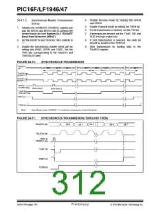
24.4.1.10 Synchronous Master Reception
Set-up:
1. Initialize the SPxBRGH, SPxBRGL register pair
for the appropriate baud rate. Set or clear the
BRGH and BRG16 bits, as required, to achieve
the desired baud rate.
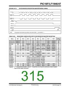
To initiate reception, set either SREN or CREN. Data is
sampled at the RXx/DTx pin on the trailing edge of the
TXx/CKx clock pin and is shifted into the Receive Shift
Register (RSR). When a complete character is
received into the RSR, the RCxIF bit is set and the
character is automatically transferred to the two
character receive FIFO. The Least Significant eight bits
of the top character in the receive FIFO are available in
RCxREG. The RCxIF bit remains set as long as there
are un-read characters in the receive FIFO.
2. Set the RXx/DTx and TXx/CKx TRIS controls to
‘1’.
3. Enable the synchronous master serial port by
setting bits SYNC, SPEN and CSRC. Disable
RXx/DTx and TXx/CKx output drivers by setting
the corresponding TRIS bits.
4. Ensure bits CREN and SREN are clear.
5. If using interrupts, set the GIE and PEIE bits of
the INTCON register and set RCxIE.
24.4.1.7
Slave Clock
6. If 9-bit reception is desired, set bit RX9.
Synchronous data transfers use a separate clock line,
which is synchronous with the data. A device configured
as a slave receives the clock on the TXx/CKx line. The
TXx/CKx pin output driver must be disabled by setting
the associated TRIS bit when the device is configured
for synchronous slave transmit or receive operation.
Serial data bits change on the leading edge to ensure
they are valid at the trailing edge of each clock. One data
bit is transferred for each clock cycle. Only as many
clock cycles should be received as there are data bits.
7. Start reception by setting the SREN bit or for
continuous reception, set the CREN bit.
8. Interrupt flag bit RCxIF will be set when recep-
tion of a character is complete. An interrupt will
be generated if the enable bit RCxIE was set.
9. Read the RCxSTA register to get the ninth bit (if
enabled) and determine if any error occurred
during reception.
10. Read the 8-bit received data by reading the
RCxREG register.
24.4.1.8
Receive Overrun Error
11. If an overrun error occurs, clear the error by
either clearing the CREN bit of the RCxSTA
register or by clearing the SPEN bit which resets
the EUSART.
The receive FIFO buffer can hold two characters. An
overrun error will be generated if a third character, in its
entirety, is received before RCxREG is read to access
the FIFO. When this happens the OERR bit of the
RCxSTA register is set. Previous data in the FIFO will
not be overwritten. The two characters in the FIFO
buffer can be read, however, no additional characters
will be received until the error is cleared. The OERR bit
can only be cleared by clearing the overrun condition.
If the overrun error occurred when the SREN bit is set
and CREN is clear then the error is cleared by reading
RCxREG.
DS41414A-page 312
Preliminary
2010 Microchip Technology Inc.

 MICROCHIP [ MICROCHIP ]