PIC16F/LF1946/47
24.4.2.3
EUSART Synchronous Slave
Reception
24.4.2.4
Synchronous Slave Reception
Set-up:
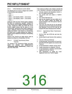
The operation of the Synchronous Master and Slave
modes is identical (Section 24.4.1.6 “Synchronous
Master Reception”), with the following exceptions:
1. Set the SYNC and SPEN bits and clear the
CSRC bit.
2. Set the RXx/DTx and TXx/CKx TRIS controls to
‘1’.
• Sleep
3. If using interrupts, ensure that the GIE and PEIE
bits of the INTCON register are set and set the
RCxIE bit.
• CREN bit is always set, therefore the receiver is
never Idle
• SREN bit, which is a “don’t care” in Slave mode
4. If 9-bit reception is desired, set the RX9 bit.
5. Set the CREN bit to enable reception.
A character may be received while in Sleep mode by
setting the CREN bit prior to entering Sleep. Once the
word is received, the RSR register will transfer the data
to the RCxREG register. If the RCxIE enable bit is set,
the interrupt generated will wake the device from Sleep
and execute the next instruction. If the GIE bit is also
set, the program will branch to the interrupt vector.
6. The RCxIF bit will be set when reception is
complete. An interrupt will be generated if the
RCxIE bit was set.
7. If 9-bit mode is enabled, retrieve the Most
Significant bit from the RX9D bit of the RCxSTA
register.
8. Retrieve the 8 Least Significant bits from the
receive FIFO by reading the RCxREG register.
9. If an overrun error occurs, clear the error by
either clearing the CREN bit of the RCxSTA
register or by clearing the SPEN bit which resets
the EUSART.
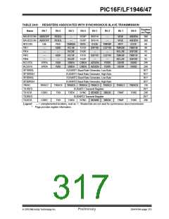
TABLE 24-10: REGISTERS ASSOCIATED WITH SYNCHRONOUS SLAVE RECEPTION
Register
on Page
Name
Bit 7
Bit 6
Bit 5
Bit 4
Bit 3
Bit 2
Bit 1
Bit 0
BAUD1CON
BAUD2CON
INTCON
PIE1
ABDOVF
RCIDL
RCIDL
PEIE
ADIE
—
—
SCKP
SCKP
INTE
BRG16
BRG16
IOCIE
SSP1IE
—
—
—
WUE
WUE
ABDEN
ABDEN
IOCIF
300
300
89
ABDOVF
—
GIE
—
TMR0IE
RC1IE
RC2IE
RC1IF
RC2IF
TMR0IF
CCP1IE
—
INTF
TX1IE
TX2IE
TX1IF
TX2IF
TMR2IE
BCL2IE
TMR2IF
BCL2IF
TMR1IE
SSP2IE
TMR1IF
SSP2IF
90
PIE4
—
93
PIR1
—
ADIF
—
SSP1IF
—
CCP1IF
—
94
PIR4
—
93
RC1REG
RC1STA
RC2REG
RC2STA
SP1BRGL
SP1BRGH
SP2BRGL
SP2BRGH
TX1STA
TX2STA
EUSART1 Receive Register
CREN ADDEN
EUSART2 Receive Register
CREN ADDEN
294*
299
294*
299
301*
301*
301*
301*
298
298
SPEN
SPEN
RX9
RX9
SREN
FERR
OERR
OERR
RX9D
RX9D
SREN
FERR
EUSART1 Baud Rate Generator, Low Byte
EUSART1 Baud Rate Generator, High Byte
EUSART2 Baud Rate Generator, Low Byte
EUSART2 Baud Rate Generator, High Byte
CSRC
CSRC
TX9
TX9
TXEN
TXEN
SYNC
SYNC
SENDB
SENDB
BRGH
BRGH
TRMT
TRMT
TX9D
TX9D
Legend: — = unimplemented locations, read as ‘0’. Shaded bits are not used for synchronous slave reception.
Page provides register information.
*
DS41414A-page 316
Preliminary
2010 Microchip Technology Inc.

 MICROCHIP [ MICROCHIP ]