PIC16F/LF1946/47
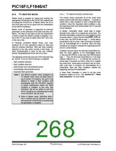
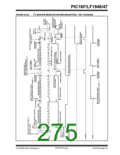
23.6.6 I2C MASTER MODE TRANSMISSION
23.6.6.3
ACKSTAT Status Flag
In Transmit mode, the ACKSTAT bit of the SSPxCON2
register is cleared when the slave has sent an Acknowl-
edge (ACK = 0) and is set when the slave does not
Acknowledge (ACK = 1). A slave sends an Acknowl-
edge when it has recognized its address (including a
general call), or when the slave has properly received
its data.
Transmission of a data byte, a 7-bit address or the
other half of a 10-bit address is accomplished by simply
writing a value to the SSPxBUF register. This action will
set the Buffer Full flag bit, BF, and allow the Baud Rate
Generator to begin counting and start the next trans-
mission. Each bit of address/data will be shifted out
onto the SDAx pin after the falling edge of SCLx is
asserted. SCLx is held low for one Baud Rate Genera-
tor rollover count (TBRG). Data should be valid before
SCLx is released high. When the SCLx pin is released
high, it is held that way for TBRG. The data on the SDAx
pin must remain stable for that duration and some hold
time after the next falling edge of SCLx. After the eighth
bit is shifted out (the falling edge of the eighth clock),
the BF flag is cleared and the master releases SDAx.
This allows the slave device being addressed to
respond with an ACK bit during the ninth bit time if an
address match occurred, or if data was received prop-
erly. The status of ACK is written into the ACKSTAT bit
on the rising edge of the ninth clock. If the master
receives an Acknowledge, the Acknowledge Status bit,
ACKSTAT, is cleared. If not, the bit is set. After the ninth
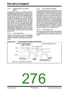
clock, the SSPxIF bit is set and the master clock (Baud
Rate Generator) is suspended until the next data byte
is loaded into the SSPxBUF, leaving SCLx low and
SDAx unchanged (Figure 23-27).
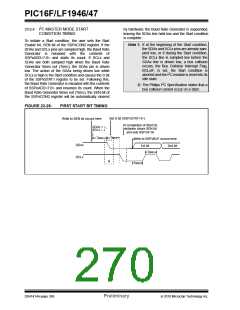
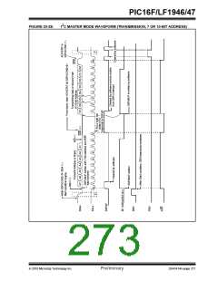
23.6.6.4 Typical transmit sequence:
1. The user generates a Start condition by setting
the SEN bit of the SSPxCON2 register.
2. SSPxIF is set by hardware on completion of the
Start.
3. SSPxIF is cleared by software.
4. The MSSPx module will wait the required start
time before any other operation takes place.
5. The user loads the SSPxBUF with the slave
address to transmit.
6. Address is shifted out the SDAx pin until all 8 bits
are transmitted. Transmission begins as soon
as SSPxBUF is written to.
7. The MSSPx module shifts in the ACK bit from
the slave device and writes its value into the
ACKSTAT bit of the SSPxCON2 register.
8. The MSSPx module generates an interrupt at
the end of the ninth clock cycle by setting the
SSPxIF bit.
After the write to the SSPxBUF, each bit of the address
will be shifted out on the falling edge of SCLx until all
seven address bits and the R/W bit are completed. On
the falling edge of the eighth clock, the master will
release the SDAx pin, allowing the slave to respond
with an Acknowledge. On the falling edge of the ninth
clock, the master will sample the SDAx pin to see if the
address was recognized by a slave. The status of the
ACK bit is loaded into the ACKSTAT Status bit of the
SSPxCON2 register. Following the falling edge of the
ninth clock transmission of the address, the SSPxIF is
set, the BF flag is cleared and the Baud Rate Generator
is turned off until another write to the SSPxBUF takes
place, holding SCLx low and allowing SDAx to float.
9. The user loads the SSPxBUF with eight bits of
data.
10. Data is shifted out the SDAx pin until all 8 bits
are transmitted.
11. The MSSPx module shifts in the ACK bit from
the slave device and writes its value into the
ACKSTAT bit of the SSPxCON2 register.
12. Steps 8-11 are repeated for all transmitted data
bytes.
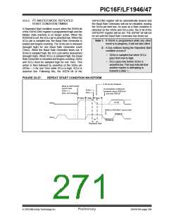
13. The user generates a Stop or Restart condition
by setting the PEN or RSEN bits of the
SSPxCON2 register. Interrupt is generated once
the Stop/Restart condition is complete.
23.6.6.1
BF Status Flag
In Transmit mode, the BF bit of the SSPxSTAT register
is set when the CPU writes to SSPxBUF and is cleared
when all 8 bits are shifted out.
23.6.6.2
WCOL Status Flag
If the user writes the SSPxBUF when a transmit is
already in progress (i.e., SSPxSR is still shifting out a
data byte), the WCOL is set and the contents of the
buffer are unchanged (the write doesn’t occur).
WCOL must be cleared by software before the next
transmission.
DS41414A-page 270
Preliminary
2010 Microchip Technology Inc.

 MICROCHIP [ MICROCHIP ]