PIC16F/LF1946/47
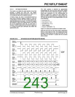
23.2.6 SPI OPERATION IN SLEEP MODE
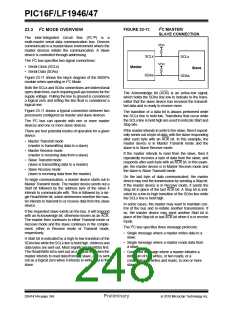
In SPI Master mode, when the Sleep mode is selected,
all module clocks are halted and the transmis-
sion/reception will remain in that state until the device
wakes. After the device returns to Run mode, the mod-
ule will resume transmitting and receiving data.
In SPI Master mode, module clocks may be operating
at a different speed than when in full power mode; in
the case of the Sleep mode, all clocks are halted.
Special care must be taken by the user when the
MSSPx clock is much faster than the system clock.
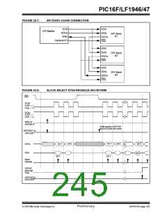
In SPI Slave mode, the SPI Transmit/Receive Shift
register operates asynchronously to the device. This
allows the device to be placed in Sleep mode and data
to be shifted into the SPI Transmit/Receive Shift
register. When all 8 bits have been received, the
MSSPx interrupt flag bit will be set and if enabled, will
wake the device.
In Slave mode, when MSSPx interrupts are enabled,
after the master completes sending data, an MSSPx
interrupt will wake the controller from Sleep.
If an exit from Sleep mode is not desired, MSSPx inter-
rupts should be disabled.
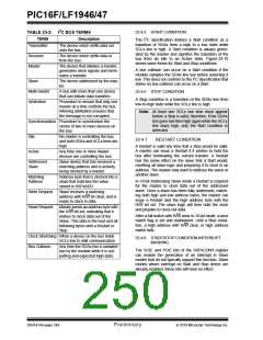
TABLE 23-1: SUMMARY OF REGISTERS ASSOCIATED WITH SPI OPERATION
Register
on Page
Name
Bit 7
Bit 6
Bit 5
Bit 4
Bit 3
Bit 2
Bit 1
Bit 0
ANSELA
APFCON
INTCON
PIE1
ANSA7
P3CSEL
GIE
ANSA6
P3BSEL
PEIE
ADIE
—
ANSA5
P2DSEL
TMR0IE
RCIE
ANSA4
P2CSEL
INTE
ANSA3
P2BSEL
IOCIE
SSP1IE
—
ANSA2
CCP2SEL
TMR0IF
CCP1IE
—
ANSA1
P1CSEL
INTF
ANSA0
P1BSEL
IOCIF
125
122
89
TMR1GIE
—
TXIE
TMR2IE
BCL2IE
TMR2IF
BCL2IF
TMR1IE
SSP2IE
TMR1IF
SSP2IF
90
PIE4
RC2IE
RCIF
TX2IE
TXIF
93
PIR1
TMR1GIF
—
ADIF
—
SSP1IF
—
CCP1IF
—
94
PIR4
RC2IF
TX2IF
97
SSPxBUF
SSPxCON1
Synchronous Serial Port Receive Buffer/Transmit Register
239*
284
286
283
124
127
WCOL
SSPxOV
PCIE
SSPxEN
SCIE
CKP
SSPxM<3:0>
SSPxCON3 ACKTIM
BOEN
SDAHT
SBCDE
AHEN
DHEN
SSPxSTAT
TRISA
SMP
CKE
D/A
P
S
R/W
UA
BF
TRISA7
TRISB7
TRISA6
TRISB6
TRISA5
TRISB5
TRISA4
TRISB4
TRISA3
TRISB3
TRISA2
TRISB2
TRISA1
TRISB1
TRISA0
TRISB0
TRISB
Legend:
— = Unimplemented location, read as ‘0’. Shaded cells are not used by the MSSPx in SPI mode.
*
Page provides register information.
2010 Microchip Technology Inc.
Preliminary
DS41414A-page 245

 MICROCHIP [ MICROCHIP ]