PIC16F/LF1946/47
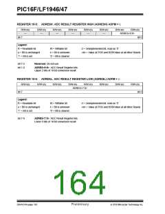
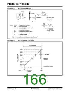
FIGURE 15-4:
ANALOG INPUT MODEL
VDD
Analog
Input
pin
Sampling
Switch
VT 0.6V
SS
RIC 1k
Rss
Rs
(1)
CPIN
5 pF
VA
I LEAKAGE
CHOLD = 10 pF
VSS/VREF-
VT 0.6V
6V
5V
RSS
VDD 4V
3V
Legend:
CHOLD
CPIN
= Sample/Hold Capacitance
= Input Capacitance
2V
I LEAKAGE = Leakage current at the pin due to
various junctions
5 6 7 8 9 1011
Sampling Switch
RIC
RSS
SS
VT
= Interconnect Resistance
= Resistance of Sampling Switch
= Sampling Switch
(k)
= Threshold Voltage
Note 1: Refer to Section 29.0 “Electrical Specifications”.
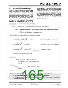
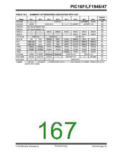
FIGURE 15-5:
ADC TRANSFER FUNCTION
Full-Scale Range
3FFh
3FEh
3FDh
3FCh
3FBh
1 LSB ideal
Full-Scale
Transition
004h
003h
002h
001h
000h
Analog Input Voltage
1 LSB ideal
Zero-Scale
Transition
VREF+
VREF-
DS41414A-page 164
Preliminary
2010 Microchip Technology Inc.

 MICROCHIP [ MICROCHIP ]