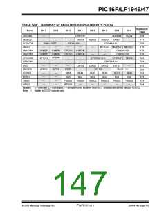
PIC16F/LF1946/47
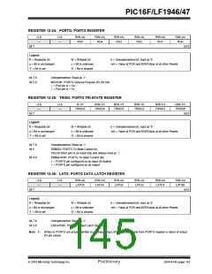
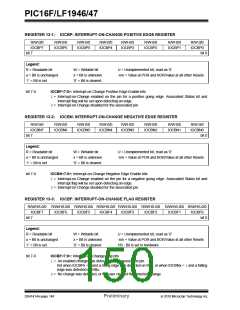
REGISTER 12-27: ANSELG: PORTG ANALOG SELECT REGISTER
U-0
—
U-0
—
U-0
—
R/W-1/1
ANSG4
R/W-1/1
ANSG3
R/W-1/1
ANSG2
R/W-1/1
ANSG1
U-0
—
bit 7
bit 0
Legend:
R = Readable bit
W = Writable bit
U = Unimplemented bit, read as ‘0’
-n/n = Value at POR and BOR/Value at all other Resets
u = Bit is unchanged
‘1’ = Bit is set
x = Bit is unknown
‘0’ = Bit is cleared
bit 7-5
bit 4-1
Unimplemented: Read as ‘0’.
ANSG<4:1>: Analog Select between Analog or Digital Function on Pins RG<4:0>, respectively
0= Digital I/O. Pin is assigned to port or digital special function.
1= Analog input. Pin is assigned as analog input(1). Digital input buffer disabled.
bit 0
Unimplemented: Read as ‘0’.
Note 1: When setting a pin to an analog input, the corresponding TRIS bit must be set to Input mode in order to
allow external control of the voltage on the pin.
REGISTER 12-28: WPUG: WEAK PULL-UP PORTB REGISTER
U-0
—
U-0
—
R/W-1/1
WPUG5
U-0
—
U-0
—
U-0
—
U-0
—
U-0
—
bit 7
bit 0
Legend:
R = Readable bit
u = Bit is unchanged
‘1’ = Bit is set
W = Writable bit
x = Bit is unknown
‘0’ = Bit is cleared
U = Unimplemented bit, read as ‘0’
-n/n = Value at POR and BOR/Value at all other Resets
bit 7-6
bit 5
Unimplemented: Read as ‘0’.
WPUG5: Weak Pull-up Register bits
1= Pull-up enabled
0= Pull-up disabled
bit 4-0
Unimplemented: Read as ‘0’.
Note 1: Global WPUEN bit of the OPTION register must be cleared for individual pull-ups to be enabled.
2: The weak pull-up device is automatically disabled if the pin is in configured as an output.
DS41414A-page 144
Preliminary
2010 Microchip Technology Inc.

 MICROCHIP [ MICROCHIP ]