PIC16F/LF1946/47
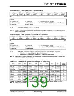
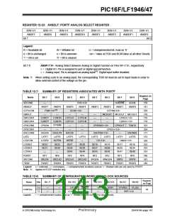
REGISTER 12-23: ANSELF: PORTF ANALOG SELECT REGISTER
R/W-1/1
ANSF7
R/W-1/1
ANSF6
R/W-1/1
ANSF5
R/W-1/1
ANSDF4
R/W-1/1
ANSF3
R/W-1/1
ANSF2
R/W-1/1
ANSDF1
R/W-1/1
ANSF0
bit 7
bit 0
Legend:
R = Readable bit
W = Writable bit
U = Unimplemented bit, read as ‘0’
-n/n = Value at POR and BOR/Value at all other Resets
u = Bit is unchanged
‘1’ = Bit is set
x = Bit is unknown
‘0’ = Bit is cleared
bit 7-0
ANSF<7:0>: Analog Select between Analog or Digital Function on Pins RF<7:0>, respectively
0= Digital I/O. Pin is assigned to port or digital special function.
1= Analog input. Pin is assigned as analog input(1). Digital input buffer disabled.
Note 1: When setting a pin to an analog input, the corresponding TRIS bit must be set to Input mode in order to
allow external control of the voltage on the pin.
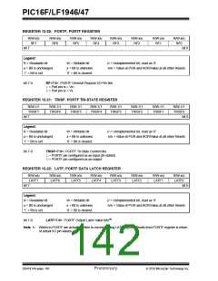
TABLE 12-7: SUMMARY OF REGISTERS ASSOCIATED WITH PORTF
Registeron
Name
Bit 7
Bit 6
Bit 5
Bit 4
Bit 3
Bit 2
Bit 1
Bit 0
Page
ADCON0
ANSELF
CCPxCON
CMOUT
—
CHS<4:0>
ANSF4
GO/DONE
ANSF1
ADON
159
141
229
179
179
179
323
324
171
133
329
333
333
333
ANSF7
ANSF6
ANSF5
ANSF3
ANSF2
ANSF0
(1)
PxM<1:0>
DCxB<1:0>
CCPxM<3:0>
MC3OUT MC2OUT MC1OUT
—
—
—
C1PCH1
C2PCH1
—
—
C1PCH0
C2PCH0
—
—
—
—
CM1CON1
CM2CON1
CPSCON0
CPSCON1
DACCON0
LATD
C1INTP
C2INTP
CPSON
—
C1INTN
C2INTN
CPSRM
—
—
C1NCH<1:0>
C2NCH<1:0>
CPSRNG<1:0>
CPSOUT
T0XCS
—
—
—
CPSCH<3:0>
DACEN
LATF7
LCDEN
SE23
DACLPS
LATF6
SLPEN
SE22
DACOE
LATF5
WERR
SE21
SE29
SE45
—
DACPSS<1:0>
LATF3 LATF2
CS<1:0>
SE19
—
DACNSS
LATF0
LATF4
—
LATF1
LCDCON
LCDSE2
LCDSE3
LCDSE5
LMUX<1:0>
SE20
SE28
SE44
SE18
SE26
SE42
SE17
SE25
SE41
SE16
SE24
SE40
SE31
SE30
SE27
SE43
—
—
PORTF
SRCON0
TRISF
RF7
RF6
RF5
RF4
RF3
RF2
RF1
RF0
140
183
140
SRLEN
TRISF7
SRCLK2
TRISF6
SRCLK1
TRISF5
SRCLK0
TRISF4
SRQEN
TRISF3
SRNQEN
TRISF2
SRPS
TRISF1
SRPR
TRISF0
Legend:
x= unknown, u= unchanged, – = unimplemented locations read as ‘0’. Shaded cells are not used by PORTF.
Note 1: Applies to ECCP modules only.
TABLE 12-8: SUMMARY OF CONFIGURATION WORD WITH CLOCK SOURCES
Register
on Page
Name
Bits
Bit -/7
Bit -/6
Bit 13/5
Bit 12/4
Bit 11/3
Bit 10/2
Bit 9/1
Bit 8/0
13:8
7:0
—
—
—
—
LVP
DEBUG
—
—
—
BORV
—
STVREN
PLLEN
CONFIG2
56
VCAPEN
WRT<1:0>
Legend:
— = unimplemented location, read as ‘0’. Shaded cells are not used by clock sources.
2010 Microchip Technology Inc.
Preliminary
DS41414A-page 141

 MICROCHIP [ MICROCHIP ]