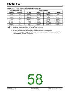
PIC12F683
9.1.7
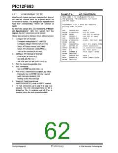
CONFIGURING THE A/D
EXAMPLE 9-1:
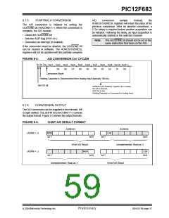
A/D CONVERSION
;This code block configures the A/D
;for polling, Vdd reference, R/C clock
;and GP0 input.
;
;Conversion start & wait for complete
;polling code included.
;
After the A/D module has been configured as desired,
the selected channel must be acquired before the
conversion is started. The analog input channels must
have their corresponding TRISIO bits selected as
inputs.
To determine sample time, see Section 15.0 “Electri-
cal Specifications”. After this sample time has
elapsed, the A/D conversion can be started.
BSF
STATUS,RP0
;Bank 1
MOVLW B’01110001’
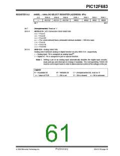
MOVWF ANSEL
;A/D RC clock
;Set GP0 to analog
;Set GP0 to input
;Bank 0
These steps should be followed for an A/D conversion:
BSF
BCF
TRISIO,0
STATUS,RP0
1. Configure the A/D module:
MOVLW B’10000001’
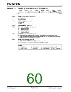
MOVWF ADCON0
;Right, Vdd Vref, AN0
• Configure analog/digital I/O (ANSEL)
• Configure voltage reference (ADCON0)
• Select A/D input channel (ADCON0)
• Select A/D conversion clock (ANSEL)
• Turn on A/D module (ADCON0)
2. Configure A/D interrupt (if desired):
• Clear ADIF bit (PIR1<6>)
CALL
BSF
SampleTime
ADCON0,GO
;Wait min sample time
;Start conversion
;Is conversion done?
;No, test again
BTFSC ADCON0,GO
GOTO
MOVF
$-1
ADRESH,W
;Read upper 2 bits
MOVWF RESULTHI
BSF
MOVF
STATUS,RP0
ADRESL,W
;Bank 1
;Read lower 8 bits
• Set ADIE bit (PIE1<6>)
MOVWF RESULTLO
• Set PEIE and GIE bits (INTCON<7:6>)
3. Wait the required acquisition time.
4. Start conversion:
• Set GO/DONE bit (ADCON0<1>)
5. Wait for A/D conversion to complete, by either:
• Polling for the GO/DONE bit to be cleared
(with interrupts disabled); OR
• Waiting for the A/D interrupt
6. Read A/D Result register pair
(ADRESH:ADRESL), clear bit ADIF if required.
7. For next conversion, go to step 1 or step 2 as
required. The A/D conversion time per bit is
defined as TAD. A minimum wait of 2 TAD is
required before the next acquisition starts.
DS41211B-page 60
Preliminary
2004 Microchip Technology Inc.

 MICROCHIP [ MICROCHIP ]