PIC12F683
If the A/D interrupt is enabled, the device awakens from
Sleep. If the GIE bit (INTCON<7>) is set, the program
counter is set to the interrupt vector (0004h); if GIE is
clear, the next instruction is executed. If the A/D inter-
rupt is not enabled, the A/D module is turned off,
although the ADON bit remains set.
9.3
A/D Operation During Sleep
The A/D converter module can operate during Sleep.
This requires the A/D clock source to be set to the
internal oscillator. When the RC clock source is
selected, the A/D waits one instruction before starting
the conversion. This allows the SLEEPinstruction to be
executed, thus eliminating much of the switching noise
from the conversion. When the conversion is complete,
the GO/DONE bit is cleared and the result is loaded
into the ADRESH:ADRESL registers.
When the A/D clock source is something other than
RC, a SLEEPinstruction causes the present conversion
to be aborted and the A/D module is turned off. The
ADON bit remains set.
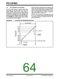
FIGURE 9-5:
PIC12F683 A/D TRANSFER FUNCTION
Full-Scale Range
3FFh
3FEh
3FDh
3FCh
3FBh
1 LSB ideal
Full-Scale
Transition
004h
003h
002h
001h
000h
Analog Input Voltage
1 LSB ideal
VREF
Zero-Scale
Transition
0V
DS41211B-page 62
Preliminary
2004 Microchip Technology Inc.

 MICROCHIP [ MICROCHIP ]