PIC12F683
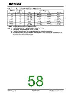
TABLE 9-1:
TAD vs. DEVICE OPERATING FREQUENCIES
Device Frequency
A/D Clock Source (TAD)
Operation
ADCS<2:0>
20 MHz
5 MHz
4 MHz
1.25 MHz
2 TOSC
4 TOSC
000
100
001
101
010
110
x11
100 ns(2)
200 ns(2)
400 ns(2)
800 ns(2)
1.6 µs
400 ns(2)
800 ns(2)
1.6 µs
500 ns(2)
1.0 µs(2)
2.0 µs
1.6 µs
3.2 µs
8 TOSC
6.4 µs
16 TOSC
32 TOSC
64 TOSC
A/D RC
3.2 µs
4.0 µs
12.8 µs(3)
25.6 µs(3)
51.2 µs(3)
2-6 µs(1,4)
6.4 µs
8.0 µs(3)
16.0 µs(3)
2-6 µs(1,4)
3.2 µs
2-6 µs(1,4)
12.8 µs(3)
2-6 µs(1,4)
Legend: Shaded cells are outside of recommended range.
Note 1: The A/D RC source has a typical TAD time of 4 µs for VDD > 3.0V.
2: These values violate the minimum required TAD time.
3: For faster conversion times, the selection of another clock source is recommended.
4: When the device frequency is greater than 1 MHz, the A/D RC clock source is only recommended if the
conversion will be performed during Sleep.
DS41211B-page 56
Preliminary
2004 Microchip Technology Inc.

 MICROCHIP [ MICROCHIP ]