PIC12F683
A/D
conversion
sample.
Instead,
the
9.1.5
STARTING A CONVERSION
ADRESH:ADRESL registers will retain the value of the
previous conversion. After an aborted conversion, a
2 TAD delay is required before another acquisition can
be initiated. Following the delay, an input acquisition is
automatically started on the selected channel.
The A/D conversion is initiated by setting the
GO/DONE bit (ADCON0<1>). When the conversion is
complete, the A/D module:
• Clears the GO/DONE bit
• Sets the ADIF flag (PIR1<6>)
• Generates an interrupt (if enabled)
Note:
The GO/DONE bit should not be set in the
same instruction that turns on the A/D.
If the conversion must be aborted, the GO/DONE bit
can be cleared in software. The ADRESH:ADRESL
registers will not be updated with the partially complete
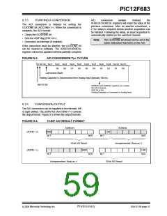
FIGURE 9-2:
A/D CONVERSION TAD CYCLES
TCY to TAD
TAD1 TAD2 TAD3 TAD4 TAD5 TAD6
TAD
7
TAD
8
TAD9 TAD10 TAD11
b9
b8
b7
b6
b5
b4
b3
b2
b1
b0
Conversion Starts
Holding Capacitor is Disconnected from Analog Input (typically 100 ns)
Set GO bit
ADRESH and ADRESL registers are Loaded,
GO bit is Cleared,
ADIF bit is Set,
Holding Capacitor is Connected to Analog Input
9.1.6
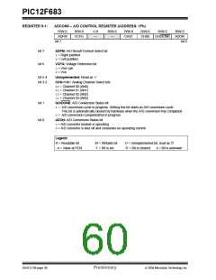
CONVERSION OUTPUT
The A/D conversion can be supplied in two formats: left
or right shifted. The ADFM bit (ADCON0<7>) controls
the output format. Figure 9-3 shows the output formats.
FIGURE 9-3:
10-BIT A/D RESULT FORMAT
ADRESH
ADRESL
LSB
(ADFM = 0)
MSB
bit 7
bit 0
bit 7
bit 0
10-bit A/D Result
Unimplemented: Read as ‘0’
(ADFM = 1)
MSB
LSB
bit 0
bit 7
bit 0
bit 7
Unimplemented: Read as ‘0’
10-bit A/D Result
2004 Microchip Technology Inc.
Preliminary
DS41211B-page 57

 MICROCHIP [ MICROCHIP ]